JAJSDW2C November 2016 – August 2021 LMS3635-Q1 , LMS3655-Q1
PRODUCTION DATA
- 1 特長
- 2 アプリケーション
- 3 概要
- 4 Revision History
- 5 Device Comparison Tables
- 6 Pin Configuration and Functions
- 7 Specifications
- 8 Detailed Description
-
9 Application and Implementation
- 9.1 Application Information
- 9.2
Typical Applications
- 9.2.1
General Application
- 9.2.1.1 Design Requirements
- 9.2.1.2 Detailed Design Procedure
- 9.2.1.3 Application Curves
- 9.2.2 Fixed 5-V Output for USB-Type Applications
- 9.2.3 Fixed 3.3-V Output
- 9.2.4 6-V Adjustable Output
- 9.2.1
General Application
- 9.3 Do's and Don't's
- 10Power Supply Recommendations
- 11Layout
- 12Device and Documentation Support
- 13Mechanical, Packaging, and Orderable Information
パッケージ・オプション
メカニカル・データ(パッケージ|ピン)
- RNL|22
サーマルパッド・メカニカル・データ
- RNL|22
発注情報
11.1 Layout Guidelines
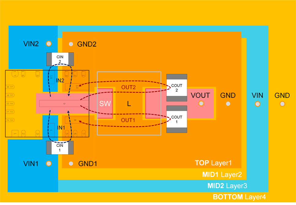
The PCB layout of a DC-DC converter is critical for optimal performance of the application. For a buck converter the input loop formed by the input capacitors and power grounds are very critical. The input loop carries fast transient currents that cause larger transient voltages when reacting with a parasitic loop inductance. The IC uses two input loops in parallel IN1 and IN2 as shown in Figure 11-1 that cuts the parasitic input inductance in half. To get the minimum input loop area two small high frequency capacitors CIN1 and CIN2 are placed as close as possible.
To further reduce inductance, an input current return path should be placed underneath the loops IN1 and IN2. The closest metal plane is MID1 Layer2, and there is a solid copper plane placed right under the IN1 and IN2 loop the parasitic loop inductance is minimized. Connecting this MID1 Layer2 plane to GND provides a nice bridge connection between GND1 and GND2 as well. Minimizing the parasitic input loop inductance will minimize switch node ringing and EMI.
The output current loop can be optimized as well by using two ceramic output caps COUT1 and COUT2, one on each side. They form two parallel ground return paths OUT1 from COUT1 back to the low-side FET PGND1 pins 5, 6, 7, 8, and a second symmetric ground return path OUT2 from COUT2 back to low-side FET PGND2 pins 10, 11, 12, and 13. Having two parallel ground return paths yield reduced ground bouncing and reduced sensitivity of surrounding circuits.
 Figure 11-1 Layout of the Power Components and Current Flow
Providing adequate thermal paths to dissipate heat is critical for operation at full current. The recommended method for heat dissipation is to use large solid 2-oz copper planes well connected to the power pins VIN1, VIN2, GND1, and GND2 which transfer the heat out of the IC over the TOP Layer1 copper planes. It is important to leave the TOP Layer1 copper planes as unbroken as possible so that heat is not trapped near the IC. The heat flow can be further optimized by thermally connecting the TOP Layer1 plane to large BOTTOM Layer 4 2-oz copper planes with vias. MID2 Layer3 is then open for all other signal routing. A fully filled or solid BOTTOM Layer4 ground plane without any interruptions or ground splitting is beneficial for EMI as well. Most important for low EMI is to use the smallest possible switch node copper area. The switch node including the CBOOT cap has the largest dV/dt signal causing common-mode noise coupling. Using any kind of grounded shield around the switch node shortens and reduces this e-field.
All these DC-DC converter descriptions can be transformed into layout guidelines:
- Place two 0.047-µF, 50-V high frequency input capacitors CIN1 and CIN2 as close as possible to the VIN1, VIN2, PGND1, PGND2 pins to minimize switch node ringing.
- Place bypass capacitors for VCC and BIAS close to their respective pins. Make sure AGND pin sees the CVCC and CBIAS capacitors first before a connection to PGND.
- Place CBOOT capacitor with smallest parasitic loop. Shielding the CBOOT capacitor and switch node has the biggest impact to reduce common-mode noise. Placing a small RBOOT resistor (less than 3 Ω is recommended) in series to CBOOT slows down the dV/dt of the switch node and reduce EMI.
- Place the feedback resistor divider for adjustable parts as close as possible to the FB pin and to AGND pin of the device. Use a dedicated feedback trace, and route away from switch node and CBOOT capacitor to avoid any cross coupling into sensitive analog feedback.
- Use a dedicated BIAS trace to avoid noise into feedback trace.
- Use a 3-Ω to 5-Ω resistor between the output and BIAS if the load is far from the output of the converter or inductive shorts on the output are possible.
- Use well connected large 2-oz. TOP and BOTTOM copper planes for all power pins VIN1/2 and PGND1/2.
- Minimize switch node and CBOOT area for lowest EMI common mode noise.
- Place input and output wires on the same side of the PCB using an EMI filter and away from the switch node for lowest EMI.
The resources in Section 12 provide additional important guidelines.