SLVS582I April 2006 – November 2014 LP2950 , LP2951
PRODUCTION DATA.
- 1 Features
- 2 Applications
- 3 Description
- 4 Revision History
- 5 Pin Configuration and Functions
- 6 Specifications
- 7 Detailed Description
- 8 Application and Implementation
- 9 Power Supply Recommendations
- 10Layout
- 11Device and Documentation Support
- 12Mechanical, Packaging, and Orderable Information
パッケージ・オプション
メカニカル・データ(パッケージ|ピン)
サーマルパッド・メカニカル・データ
- DRG|8
発注情報
8 Application and Implementation
NOTE
Information in the following applications sections is not part of the TI component specification, and TI does not warrant its accuracy or completeness. TI’s customers are responsible for determining suitability of components for their purposes. Customers should validate and test their design implementation to confirm system functionality.
8.1 Application Information
The LP295x devices are used as low-dropout regulators with a wide range of input voltages.
8.2 Typical Application
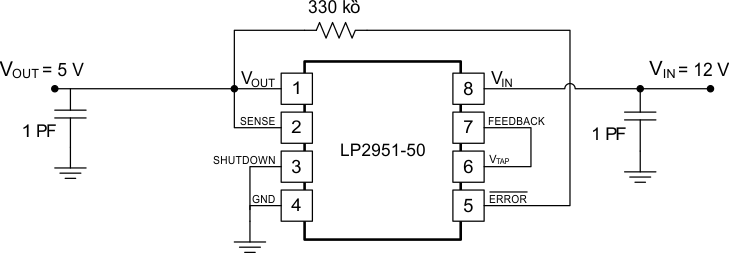 Figure 33. 12-V to 5-V Converter
8.2.1 Design Requirements
8.2.1.1 Input Capacitor (CIN)
A 1-μF (tantalum, ceramic, or aluminum) electrolytic capacitor should be placed locally at the input of the LP2950 or LP2951 device if there is, or will be, significant impedance between the ac filter capacitor and the input; for example, if a battery is used as the input or if the ac filter capacitor is located more than 10 in away. There are no ESR requirements for this capacitor, and the capacitance can be increased without limit.
8.2.1.2 Output Capacitor (COUT)
As with most PNP LDOs, stability conditions require the output capacitor to have a minimum capacitance and an ESR that falls within a certain range.
8.2.2 Detailed Design Procedure
8.2.2.1 Capacitance Value
For VOUT ≥ 5 V, a minimum of 1 μF is required. For lower VOUT, the regulator’s loop gain is running closer to unity gain and, thus, has lower phase margins. Consequently, a larger capacitance is needed for stability.
For VOUT = 3 V or 3.3 V, a minimum of 2.2 μF is recommended. For worst case, VOUT = 1.23 V (using the ADJ version), a minimum of 3.3 μF is recommended. COUT can be increased without limit and only improves the regulator stability and transient response. Regardless of its value, the output capacitor should have a resonant frequency greater than 500 kHz.
The minimum capacitance values given above are for maximum load current of 100 mA. If the maximum expected load current is less than 100 mA, then lower values of COUT can be used. For instance, if IOUT < 10 mA, then only 0.33 μF is required for COUT. For IOUT < 1 mA, 0.1 μF is sufficient for stability requirements. Thus, for a worst-case condition of 100-mA load and VOUT = VREF = 1.235 V (representing the highest load current and lowest loop gain), a minimum COUT of 3.3 μF is recommended.
For the LP2950/51, no load stability is inherent in the design — a desirable feature in CMOS circuits that are put in standby (such as RAM keep-alive applications). If the LP2951 is used with external resistors to set the output voltage, a minimum load current of 1 μA is recommended through the resistor divider.
8.2.2.2 Capacitor Types
Most tantalum or aluminum electrolytics are suitable for use at the input. Film-type capacitors also work but at higher cost. When operating at low temperature, care should be taken with aluminum electrolytics, as their electrolytes often freeze at –30°C. For this reason, solid tantalum capacitors should be used at temperatures below –25°C.
Ceramic capacitors can be used, but due to their low ESR (as low as 5 mΩ to 10 mΩ), they may not meet the minimum ESR requirement previously discussed. If a ceramic capacitor is used, a series resistor between
0.1 Ω to 2 Ω must be added to meet the minimum ESR requirement. In addition, ceramic capacitors have one glaring disadvantage that must be taken into account — a poor temperature coefficient, where the capacitance can vary significantly with temperature. For instance, a large-value ceramic capacitor (≥ 2.2 μF) can lose more than half of its capacitance as temperature rises from 25°C to 85°C. Thus, a 2.2-μF capacitor at 25°C drops well below the minimum COUT required for stability as ambient temperature rises. For this reason, select an output capacitor that maintains the minimum 2.2 μF required for stability for the entire operating temperature range.
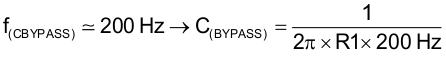
8.2.2.3 CBYPASS: Noise and Stability Improvement
In the LP2951 device, an external FEEDBACK pin directly connected to the error amplifier noninverting input can allow stray capacitance to cause instability by shunting the error amplifier feedback to GND, especially at high frequencies. This is worsened if high-value external resistors are used to set the output voltage, because a high resistance allows the stray capacitance to play a more significant role; i.e., a larger RC time delay is introduced between the output of the error amplifier and its FEEDBACK input, leading to more phase shift and lower phase margin. A solution is to add a 100-pF bypass capacitor (CBYPASS) between OUTPUT and FEEDBACK; because CBYPASS is in parallel with R1, it lowers the impedance seen at FEEDBACK at high frequencies, in effect offsetting the effect of the parasitic capacitance by providing more feedback at higher frequencies. More feedback forces the error amplifier to work at a lower loop gain, so COUT should be increased to a minimum of 3.3 μF to improve the regulator’s phase margin.
CBYPASS can be also used to reduce output noise in the LP2951 device. This bypass capacitor reduces the closed loop gain of the error amplifier at the high frequency, so noise no longer scales with the output voltage. This improvement is more noticeable with higher output voltages, where loop gain reduction is greatest. A suitable CBYPASS is calculated as shown in Equation 2:
On the 3-pin LP2950 device, noise reduction can be achieved by increasing the output capacitor, which causes the regulator bandwidth to be reduced, thus eliminating high-frequency noise. However, this method is relatively inefficient, as increasing COUT from 1 μF to 220 μF only reduces the regulator’s output noise from
430 μV to 160 μV (over a 100-kHz bandwidth).
8.2.2.4 ESR Range
The regulator control loop relies on the ESR of the output capacitor to provide a zero to add sufficient phase margin to ensure unconditional regulator stability; this requires the closed-loop gain to intersect the open-loop response in a region where the open-loop gain rolls off at 20 dB/decade. This ensures that the phase is always less than 180° (phase margin greater than 0°) at unity gain. Thus, a minimum-maximum range for the ESR must be observed.
The upper limit of this ESR range is established by the fact that an ESR that is too high could result in the zero occurring too soon, causing the gain to roll off too slowly. This, in turn, allows a third pole to appear before unity gain and introduces enough phase shift to cause instability. This typically limits the maximum ESR to approximately 5 Ω.
Conversely, the lower limit of the ESR range is tied to the fact that an ESR that is too low shifts the zero too far out, past unity gain, which allows the gain to roll off at 40 dB/decade at unity gain, resulting in a phase shift of greater than 180°. Typically, this limits the minimum ESR to approximately 20 mΩ to 30 mΩ.
For specific ESR requirements, see Typical Characteristics.
8.2.3 Application Curves
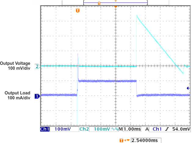 Figure 34. Load Transient Response vs Time (VOUT = 5 V, CL = 1 µF)