SBOS450C July 2009 – August 2014 OPA1611 , OPA1612
PRODUCTION DATA.
8 Application and Implementation
8.1 Application Information
The OPA1611 and OPA1612 are unity-gain stable, precision op amps with very low noise; these devices are also free from output phase reversal. Applications with noisy or high-impedance power supplies require decoupling capacitors close to the device power-supply pins. In most cases, 0.1-μF capacitors are adequate.
8.2 Noise Performance
Figure 32 shows the total circuit noise for varying source impedances with the op amp in a unity-gain configuration (no feedback resistor network, and therefore no additional noise contributions).
The OPA1611 (GBW = 40 MHz, G = +1) is shown with total circuit noise calculated. The op amp itself contributes both a voltage noise component and a current noise component. The voltage noise is commonly modeled as a time-varying component of the offset voltage. The current noise is modeled as the time-varying component of the input bias current and reacts with the source resistance to create a voltage component of noise. Therefore, the lowest noise op amp for a given application depends on the source impedance. For low source impedance, current noise is negligible, and voltage noise generally dominates. The low voltage noise of the OPA161x series op amps makes them a good choice for use in applications where the source impedance is less than 1 kΩ.
8.2.1 Detailed Design Procedure
The equation in Figure 32 shows the calculation of the total circuit noise, with these parameters:
- en = voltage noise
- In = current noise
- RS = source impedance
- k = Boltzmann’s constant = 1.38 × 10⁻²³ J/K
- T = temperature in degrees Kelvin (K)
8.2.2 Application Curve
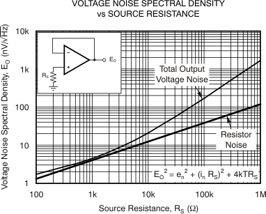 Figure 32. Noise Performance of the OPA1611 In Unity-Gain Buffer Configuration
8.2.3 Basic Noise Calculations
Design of low-noise op amp circuits requires careful consideration of a variety of possible noise contributors: noise from the signal source, noise generated in the op amp, and noise from the feedback network resistors. The total noise of the circuit is the root-sum-square combination of all noise components.
The resistive portion of the source impedance produces thermal noise proportional to the square root of the resistance. Figure 32 plots this function. The source impedance is usually fixed; consequently, select the op amp and the feedback resistors to minimize the respective contributions to the total noise.
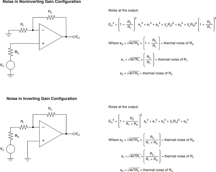
Figure 33 shows both inverting and noninverting op amp circuit configurations with gain. In circuit configurations with gain, the feedback network resistors also contribute noise.
The current noise of the op amp reacts with the feedback resistors to create additional noise components. The feedback resistor values can generally be chosen to make these noise sources negligible. The equations for total noise are shown for both configurations.
8.3 Total Harmonic Distortion Measurements
The OPA161x series op amps have excellent distortion characteristics. THD + noise is below 0.00008% (G = +1, VO = 3 VRMS, BW = 80 kHz) throughout the audio frequency range, 20 Hz to 20 kHz, with a 2-kΩ load (see Figure 7 for characteristic performance).
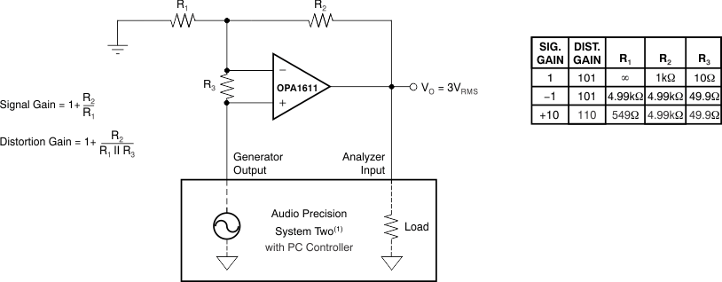
The distortion produced by OPA1611 series op amps is below the measurement limit of many commercially available distortion analyzers. However, a special test circuit (such as Figure 34 shows) can be used to extend the measurement capabilities.
Op amp distortion can be considered an internal error source that can be referred to the input. Figure 34 shows a circuit that causes the op amp distortion to be 101 times (or approximately 40 dB) greater than that normally produced by the op amp. The addition of R3 to the otherwise standard noninverting amplifier configuration alters the feedback factor or noise gain of the circuit. The closed-loop gain is unchanged, but the feedback available for error correction is reduced by a factor of 101, thus extending the resolution by 101. Note that the input signal and load applied to the op amp are the same as with conventional feedback without R3. Keep the value of R3 small to minimize its effect on the distortion measurements.
Validity of this technique can be verified by duplicating measurements at high gain and/or high frequency where the distortion is within the measurement capability of the test equipment. Measurements for this data sheet were made with an audio precision system two distortion and noise analyzer, which greatly simplifies such repetitive measurements. The measurement technique can, however, be performed with manual distortion measurement instruments.
8.4 Capacitive Loads
The dynamic characteristics of the OPA1611 and OPA1612 have been optimized for commonly encountered gains, loads, and operating conditions. The combination of low closed-loop gain and high capacitive loads decreases the phase margin of the amplifier and can lead to gain peaking or oscillations. As a result, heavier capacitive loads must be isolated from the output. The simplest way to achieve this isolation is to add a small resistor (RS equal to 50 Ω, for example) in series with the output.
This small series resistor also prevents excess power dissipation if the output of the device becomes shorted. Figure 19 and Figure 20 illustrate graphs of Small-Signal Overshoot vs Capacitive Load for several values of RS. Also, refer to Applications Bulletin AB-028, Feedback Plots Define Op Amp AC Performance (SBOA015), available for download from the TI web site, for details of analysis techniques and application circuits.
8.5 Application Circuit
Figure 35 shows how to use the OPA1611 as an amplifier for professional audio headphones. The circuit shows the left side stereo channel. An identical circuit is used to drive the right side stereo channel.
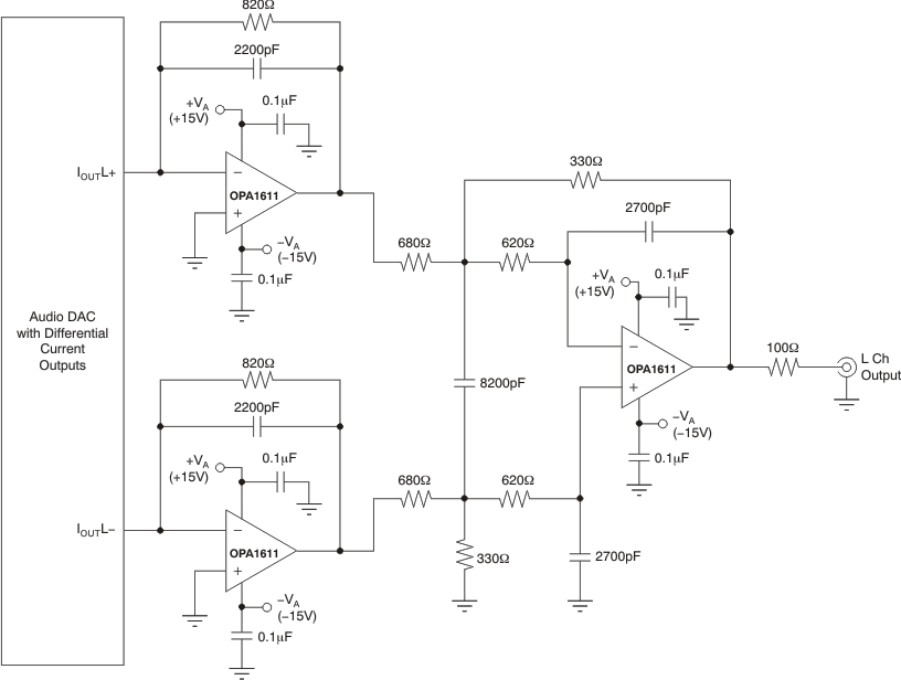 Figure 35. Audio DAC Post Filter (I/V Converter and Low-Pass Filter)