JAJSHS6D August 2019 – July 2020 OPA810
PRODUCTION DATA
- 1 特長
- 2 アプリケーション
- 3 概要
- 4 Revision History
- 5 Device Comparison Table
- 6 Pin Configuration and Functions
-
7 Specifications
- 7.1 Absolute Maximum Ratings
- 7.2 ESD Ratings
- 7.3 Recommended Operating Conditions
- 7.4 Thermal Information
- 7.5 Electrical Characteristics: 10 V
- 7.6 Electrical Characteristics: 24 V
- 7.7 Electrical Characteristics: 5 V
- 7.8 Typical Characteristics: VS = 10 V
- 7.9 Typical Characteristics: VS = 24 V
- 7.10 Typical Characteristics: VS = 5 V
- 7.11 Typical Characteristics: ±2.375-V to ±12-V Split Supply
- 8 Detailed Description
- 9 Application and Implementation
- 10Power Supply Recommendations
- 11Layout
- 12Device and Documentation Support
パッケージ・オプション
メカニカル・データ(パッケージ|ピン)
サーマルパッド・メカニカル・データ
発注情報
9.1.2 Selection of Feedback Resistors
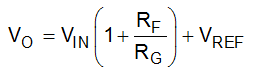
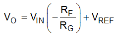
The OPA810 is a classic voltage feedback amplifier with each channel having two high-impedance inputs and a low-impedance output. Standard application circuits (as shown in Figure 9-3 and Figure 9-4) include the noninverting and inverting gain configurations. The DC operating point for each configuration is level-shifted by the reference voltage VREF which is typically set to midsupply in single-supply operation. VREF is often connected to ground in split-supply applications.
 Figure 9-3 Noninverting Amplifier
 Figure 9-4 Inverting
Amplifier
Figure 9-4 Inverting
AmplifierEquation 3 shows the closed-loop gain of an amplifier in noninverting configuration.
Equation 4 shows the closed-loop gain of an amplifier in an inverting configuration.
The magnitude of the low-frequency gain is determined by the ratio of the magnitudes of the feedback resistor (RF) and the gain setting resistor RG. The order of magnitudes of the individual values of RF and RG offer a trade-off between amplifier stability, power dissipated in the feedback resistor network, and total output noise. The feedback network increases the loading on the amplifier output. Using large values of the feedback resistors reduces the power dissipated at the amplifier output. On the other hand, this increases the inherent voltage and amplifier current noise contribution seen at the output while lowering the frequency at which a pole occurs in the feedback factor (β). This pole causes a decrease in the phase margin at zero-gain crossover frequency and potential instability. Using small feedback resistors increases power dissipation and also degrades amplifier linearity due to a heavier amplifier output load. Figure 9-5 illustrates a representative schematic of the OPA810 in an inverting configuration with the input capacitors shown.
 Figure 9-5 Inverting
Amplifier with Input Capacitors
Figure 9-5 Inverting
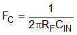
Amplifier with Input CapacitorsThe effective capacitance at the amplifier inverting input pin is shown in Equation 5, which forms a pole in β at a cut-off frequency of Equation 6.

where
- CCM is the amplifier common-mode input capacitance
- CDIFF is the amplifier differential input capacitance
- CPCB is the PCB parasitic capacitance
For low-power systems, greater the values of the feedback resistors, the earlier in frequency does the phase margin begin to reduce and cause instability. Figure 9-6 and Figure 9-7 illustrate the loop gain magnitude and phase plots, respectively, for the OPA810 simulation in TINA-TI configured as an inverting amplifier with values of feedback resistors varying by orders of magnitudes.
 Figure 9-6 Loop-Gain vs Frequency for Circuit of Figure 9-5
 Figure 9-7 Loop-Gain Phase vs Frequency for Circuit of Figure 9-5
A lower phase margin results in peaking in the frequency response and lower bandwidth as Figure 9-8 shows, which is synonymous with overshoot and ringing in the pulse response results. The OPA810 offers a flat-band voltage noise density of 6.3 nV/√ Hz. TI recommends selecting an RF so the voltage noise contribution does not exceed that of the amplifier. Figure 9-9 shows the voltage noise density variation with value of resistance at 25°C. A 2-kΩ resistor exhibits a thermal noise density of 5.75 nV/√ Hz which is comparable to the flatband noise of the OPA810. Hence, TI recommends using an RF lower than 2 kΩ while being large enough to not dissipate excessive power for the output voltage swing and supply current requirements of the application. The Section 9.1.3 section shows a detailed analysis of the various contributors to noise.
 Figure 9-8 Closed-Loop Gain vs. Frequency for Circuit of Figure 9-5
 Figure 9-9 Thermal Noise Density vs Resistance