JAJSHS6D August 2019 – July 2020 OPA810
PRODUCTION DATA
- 1 特長
- 2 アプリケーション
- 3 概要
- 4 Revision History
- 5 Device Comparison Table
- 6 Pin Configuration and Functions
-
7 Specifications
- 7.1 Absolute Maximum Ratings
- 7.2 ESD Ratings
- 7.3 Recommended Operating Conditions
- 7.4 Thermal Information
- 7.5 Electrical Characteristics: 10 V
- 7.6 Electrical Characteristics: 24 V
- 7.7 Electrical Characteristics: 5 V
- 7.8 Typical Characteristics: VS = 10 V
- 7.9 Typical Characteristics: VS = 24 V
- 7.10 Typical Characteristics: VS = 5 V
- 7.11 Typical Characteristics: ±2.375-V to ±12-V Split Supply
- 8 Detailed Description
- 9 Application and Implementation
- 10Power Supply Recommendations
- 11Layout
- 12Device and Documentation Support
パッケージ・オプション
メカニカル・データ(パッケージ|ピン)
サーマルパッド・メカニカル・データ
発注情報
9.1.1 Amplifier Gain Configurations
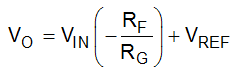
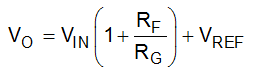
The OPA810 is a classic voltage-feedback amplifier with each channel having two high-impedance inputs and a low-impedance output. Standard application circuits (as shown in Figure 9-1 and Figure 9-2) include the noninverting and inverting gain configurations. The DC operating point for each configuration is level-shifted by the reference voltage VREF that is typically set to midsupply in single-supply operation. VREF is often connected to ground in split-supply applications.
 Figure 9-1 Noninverting Amplifier
 Figure 9-2 Inverting
Amplifier
Figure 9-2 Inverting
AmplifierEquation 1 shows the closed-loop gain of an amplifier in a noninverting configuration.
Equation 2 shows the closed-loop gain of an amplifier in an inverting configuration.