JAJSHS6D August 2019 – July 2020 OPA810
PRODUCTION DATA
- 1 特長
- 2 アプリケーション
- 3 概要
- 4 Revision History
- 5 Device Comparison Table
- 6 Pin Configuration and Functions
-
7 Specifications
- 7.1 Absolute Maximum Ratings
- 7.2 ESD Ratings
- 7.3 Recommended Operating Conditions
- 7.4 Thermal Information
- 7.5 Electrical Characteristics: 10 V
- 7.6 Electrical Characteristics: 24 V
- 7.7 Electrical Characteristics: 5 V
- 7.8 Typical Characteristics: VS = 10 V
- 7.9 Typical Characteristics: VS = 24 V
- 7.10 Typical Characteristics: VS = 5 V
- 7.11 Typical Characteristics: ±2.375-V to ±12-V Split Supply
- 8 Detailed Description
- 9 Application and Implementation
- 10Power Supply Recommendations
- 11Layout
- 12Device and Documentation Support
パッケージ・オプション
メカニカル・データ(パッケージ|ピン)
サーマルパッド・メカニカル・データ
発注情報
9.2.1.2 Detailed Design Procedure
Designs that require high bandwidth from a large area detector with relatively high transimpedance gain benefit from the low input voltage noise of the OPA810. This input voltage noise is peaked up over frequency by the diode source capacitance, and can (in many cases) become the limiting factor to input sensitivity. The key elements to the design are the expected diode capacitance (CD) with the reverse bias voltage (VBIAS) applied, the desired transimpedance gain, RF, and the GBWP for the OPA810 (70 MHz). Figure 9-12 shows a transimpedance circuit with the parameters as described in Table 9-2. With these three variables set (and including the parasitic input capacitance for the OPA810 and the printed circuit board (PCB) added to CD), the feedback capacitor value (CF) can be set to control the frequency response. The Transimpedance Considerations for High-Speed Amplifiers application report discusses using high-speed amplifiers for transimpedance applications. Set the feedback pole according to Equation 9 in order to achieve a maximally-flat second-order Butterworth frequency response:
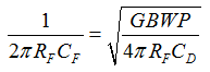
The input capacitance of the amplifier is the sum of the common-mode and differential capacitance (2.0 + 0.5) pF. The parasitic capacitance from the photodiode package and the PCB is approximately 0.3 pF. Using Equation 5 gives a total input capacitance of CD = 22.8 pF. From Equation 9, set the feedback pole at 1.55 MHz. Setting the pole at 1.55 MHz requires a total feedback capacitance of 1.03 pF.
Equation 10 shows the approximate –3-dB bandwidth of the transimpedance amplifier circuit:
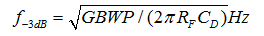
Equation 10 estimates a closed-loop bandwidth of 2.19 MHz. Figure 9-13 and Figure 9-14 show the loop-gain magnitude and phase plots from the TINA-TI simulations of the transimpedance amplifier circuit of Figure 9-12. The 1/β gain curve has a zero from RF and CIN at 70 kHz and a pole from RF and CF cancelling the 1/β zero at 1.5 MHz, resulting in a 20-dB per decade rate-of-closure at the loop-gain crossover frequency (the frequency where AOL equals 1/β), ensuring a stable circuit. A phase margin of 62° is obtained with a closed-loop bandwidth of 3 MHz and a 100-kΩ transimpedance gain.