JAJSFP5E July   2018  – February 2022 REF2025 , REF2030 , REF2033 , REF2041

PRODUCTION DATA  

  1. 特長
  2. アプリケーション
  3. 概要
  4. Revision History
  5. Device Comparison Table
  6. Pin Configuration and Functions
    1.     Pin Functions
  7. Specifications
    1. 7.1 Absolute Maximum Ratings
    2. 7.2 ESD Ratings
    3. 7.3 Recommended Operating Conditions
    4. 7.4 Thermal Information
    5. 7.5 Electrical Characteristics
    6. 7.6 Typical Characteristics
  8. Parameter Measurement Information
    1. 8.1 Solder Heat Shift
    2. 8.2 Long-Term Stability
    3. 8.3 Thermal Hysteresis
    4. 8.4 Noise Performance
  9. Detailed Description
    1. 9.1 Overview
    2. 9.2 Functional Block Diagram
    3. 9.3 Feature Description
      1. 9.3.1 VREF and VBIAS Tracking
      2. 9.3.2 Low Temperature Drift
      3. 9.3.3 Load Current
    4. 9.4 Device Functional Modes
  10. 10Applications and Implementation
    1. 10.1 Application Information
    2. 10.2 Typical Application
      1. 10.2.1 Low-Side, Current-Sensing Application
        1. 10.2.1.1 Design Requirements
        2. 10.2.1.2 Detailed Design Procedure
          1. 10.2.1.2.1 Shunt Resistor
          2. 10.2.1.2.2 Differential Amplifier
          3. 10.2.1.2.3 Voltage Reference
          4. 10.2.1.2.4 Results
        3. 10.2.1.3 Application Curves
  11. 11Power-Supply Recommendations
  12. 12Layout
    1. 12.1 Layout Guidelines
    2. 12.2 Layout Example
  13. 13Device and Documentation Support
    1. 13.1 Documentation Support
      1. 13.1.1 Related Documentation
    2. 13.2 Receiving Notification of Documentation Updates
    3. 13.3 サポート・リソース
    4. 13.4 Trademarks
    5. 13.5 Electrostatic Discharge Caution
    6. 13.6 Glossary
  14. 14Mechanical, Packaging, and Orderable Information

パッケージ・オプション

メカニカル・データ(パッケージ|ピン)
サーマルパッド・メカニカル・データ
発注情報

Power-Supply Recommendations

The REF20xx family of references feature an extremely low-dropout voltage. These references can be operated with a supply of only 20 mV above the output voltage. For loaded reference conditions, a typical dropout voltage versus load is shown in Figure 11-1. A supply bypass capacitor ranging between 0.1 µF to 10 µF is recommended.
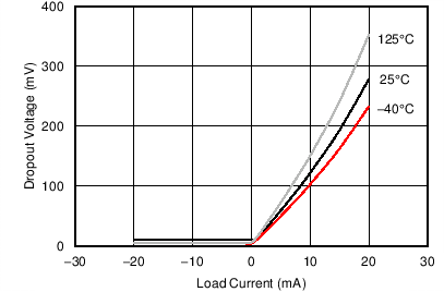
GUID-108BDC1B-0D5B-4CA0-8B64-CF7E71B0262A-low.pngFigure 11-1 Dropout Voltage vs Load Current