JAJSFP5E July 2018 – February 2022 REF2025 , REF2030 , REF2033 , REF2041
PRODUCTION DATA
- 1 特長
- 2 アプリケーション
- 3 概要
- 4 Revision History
- 5 Device Comparison Table
- 6 Pin Configuration and Functions
- 7 Specifications
- 8 Parameter Measurement Information
- 9 Detailed Description
- 10Applications and Implementation
- 11Power-Supply Recommendations
- 12Layout
- 13Device and Documentation Support
- 14Mechanical, Packaging, and Orderable Information
10.2.1.2.2 Differential Amplifier
The differential amplifier used for this design should have the following features:
- Single-supply (3 V),
- Reference voltage input,
- Low initial input offset voltage (VOS),
- Low-drift,
- Fixed gain, and
- Low-side sensing (input common-mode range below ground).
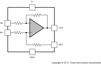
For this design, a current-shunt monitor (INA213) is used. The INA21x family topology is shown in Figure 10-3. The INA213B specifications can be found in the INA213 product data sheet.
 Figure 10-3 INA21x Current-Shunt Monitor Topology
The INA213B is an excellent choice for this application because all the required features are included. In general, instrumentation amplifiers (INAs) do not have the input common-mode swing to ground that is essential for this application. In addition, INAs require external resistors to set their gain, which is not desirable for low-drift applications. Difference amplifiers typically have larger input bias currents, which reduce solution accuracy at small load currents. Difference amplifiers typically have a gain of 1 V/V. When the gain is adjustable, these amplifiers use external resistors that are not conducive to low-drift applications.