JAJSEB5C July 2013 – January 2018 SN65HVD888
PRODUCTION DATA.
- 1 特長
- 2 アプリケーション
- 3 概要
- 4 改訂履歴
- 5 Pin Configuration and Functions
- 6 Specifications
- 7 Parameter Measurement information
- 8 Detailed Description
- 9 Application and Implementation
- 10Power Supply Recommendations
- 11Layout
- 12デバイスおよびドキュメントのサポート
- 13メカニカル、パッケージ、および注文情報
7.1 Driver
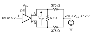
 Figure 4. Measurement of Driver Differential-Output Voltage With Common-Mode Load
 Figure 5. Measurement of Driver Differential and Common-Mode Output With RS-485 Load
 Figure 6. Measurement of Driver Differential-Output Rise and Fall Times and Propagation Delays
 Figure 7. Measurement of Driver Enable and Disable Times With Active-High Output and Pull-Down Load
 Figure 8. Measurement of Driver Enable and Disable Times With Active-Low Output and Pull-up Load