JAJSL15N July 1997 – April 2021 SN55LVDS31 , SN65LVDS31 , SN65LVDS3487 , SN65LVDS9638
PRODUCTION DATA
- 1 特長
- 2 アプリケーション
- 3 概要
- 4 Revision History
- 5 概要 (続き)
- 6 Pin Configuration and Functions
-
7 Specifications
- 7.1 Absolute Maximum Ratings #GUID-35E89C88-1E48-404C-8AB6-22CCA817C2ED/SLLS2613609
- 7.2 ESD Ratings
- 7.3 Recommended Operating Conditions
- 7.4 Thermal Information
- 7.5 Electrical Characteristics: SN55LVDS31
- 7.6 Electrical Characteristics: SN65LVDSxxxx
- 7.7 Switching Characteristics: SN55LVDS31
- 7.8 Switching Characteristics: SN65LVDSxxxx
- 7.9 Typical Characteristics
- 8 Parameter Measurement Information
- 9 Detailed Description
- 10Application and Implementation
- 11Power Supply Recommendations
- 12Layout
- 13Device and Documentation Support
- 14Mechanical, Packaging, and Orderable Information
パッケージ・オプション
デバイスごとのパッケージ図は、PDF版データシートをご参照ください。
メカニカル・データ(パッケージ|ピン)
- PW|16
- NS|16
- D|16
サーマルパッド・メカニカル・データ
- D|16
発注情報
10.1 Application Information
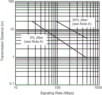
The SNx5LVDSxx devices are dual- and quad-channel LVDS drivers. These devices are generally used as building blocks for high-speed, point-to-point, data transmission where ground differences are less than 1 V. LVDS drivers and receivers provide high-speed signaling rates that are often implemented with ECL class devices without the ECL power and dual-supply requirements. A common question with any class of driver is how far and how fast can the devices operate. While individual drivers and receivers have specifications that define their inherent switching rate, a communication link will quite often be limited by the impairments introduced by the interconnecting media. Figure 10-1 shows the typical relationship between signaling rate and distance achievable depends on the quality of the eye pattern at the receiver that is either desired or needed. Figure 10-1 shows the curves representing 5% and 30% eye closure due to inter-symbol interference (ISI).

| 24 A WG UTP 96 Ω (PVC Dielectric) |