JAJSL15N July 1997 – April 2021 SN55LVDS31 , SN65LVDS31 , SN65LVDS3487 , SN65LVDS9638
PRODUCTION DATA
- 1 特長
- 2 アプリケーション
- 3 概要
- 4 Revision History
- 5 概要 (続き)
- 6 Pin Configuration and Functions
-
7 Specifications
- 7.1 Absolute Maximum Ratings #GUID-35E89C88-1E48-404C-8AB6-22CCA817C2ED/SLLS2613609
- 7.2 ESD Ratings
- 7.3 Recommended Operating Conditions
- 7.4 Thermal Information
- 7.5 Electrical Characteristics: SN55LVDS31
- 7.6 Electrical Characteristics: SN65LVDSxxxx
- 7.7 Switching Characteristics: SN55LVDS31
- 7.8 Switching Characteristics: SN65LVDSxxxx
- 7.9 Typical Characteristics
- 8 Parameter Measurement Information
- 9 Detailed Description
- 10Application and Implementation
- 11Power Supply Recommendations
- 12Layout
- 13Device and Documentation Support
- 14Mechanical, Packaging, and Orderable Information
パッケージ・オプション
デバイスごとのパッケージ図は、PDF版データシートをご参照ください。
メカニカル・データ(パッケージ|ピン)
- PW|16
- NS|16
- D|16
サーマルパッド・メカニカル・データ
- D|16
発注情報
6 Pin Configuration and Functions
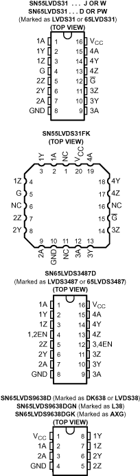
Table 6-1 Pin Functions: SN55LVDS31 J or W, SN65LVDS31 D
or PW
| PIN | I/O | DESCRIPTION | |
|---|---|---|---|
| NAME | NUMBER | ||
| VCC | 16 | – | Supply voltage |
| GND | 8 | – | Ground |
| 1A | 1 | I | LVTTL input signal |
| 1Y | 2 | O | Differential (LVDS) non-inverting output |
| 1Z | 3 | O | Differential (LVDS) inverting output |
| 2A | 7 | I | LVTTL input signal |
| 2Y | 6 | O | Differential (LVDS) non-inverting output |
| 2Z | 5 | O | Differential (LVDS) inverting output |
| 3A | 9 | I | LVTTL input signal |
| 3Y | 10 | O | Differential (LVDS) non-inverting output |
| 3Z | 11 | O | Differential (LVDS) inverting output |
| 4A | 15 | I | LVTTL input signal |
| 4Y | 14 | O | Differential (LVDS) non-inverting output |
| 4Z | 13 | O | Differential (LVDS) inverting output |
| G | 4 | I | Enable (HI = ENABLE) |
| G/ | 12 | I | Enable (LO = ENABLE) |
Table 6-2 Pin Functions: SN65LVDS31FK
| PIN | I/O | DESCRIPTION | |
|---|---|---|---|
| NAME | NUMBER | ||
| VCC | 20 | – | Supply voltage |
| GND | 10 | – | Ground |
| 1A | 2 | I | LVTTL input signal |
| 1Y | 3 | O | Differential (LVDS) non-inverting output |
| 1Z | 4 | O | Differential (LVDS) inverting output |
| 2A | 9 | I | LVTTL input signal |
| 2Y | 8 | O | Differential (LVDS) non-inverting output |
| 2Z | 7 | O | Differential (LVDS) inverting output |
| 3A | 12 | I | LVTTL input signal |
| 3Y | 13 | O | Differential (LVDS) non-inverting output |
| 3Z | 14 | O | Differential (LVDS) inverting output |
| 4A | 19 | I | LVTTL input signal |
| 4Y | 18 | O | Differential (LVDS) non-inverting output |
| 4Z | 17 | O | Differential (LVDS) inverting output |
| G | 5 | I | Enable (HI = ENABLE) |
| G/ | 15 | I | Enable (LO = ENABLE) |
| NC | 1, 6, 11, 16 | – | No connection |
Table 6-3 Pin Functions: SN65LVDS3487D
| PIN | I/O | DESCRIPTION | |
|---|---|---|---|
| NAME | NUMBER | ||
| VCC | 16 | – | Supply voltage |
| GND | 8 | – | Ground |
| 1A | 1 | I | LVTTL input signal |
| 1Y | 2 | O | Differential (LVDS) non-inverting output |
| 1Z | 3 | O | Differential (LVDS) inverting output |
| 2A | 7 | I | LVTTL input signal |
| 2Y | 6 | O | Differential (LVDS) non-inverting output |
| 2Z | 5 | O | Differential (LVDS) inverting output |
| 3A | 9 | I | LVTTL input signal |
| 3Y | 10 | O | Differential (LVDS) non-inverting output |
| 3Z | 11 | O | Differential (LVDS) inverting output |
| 4A | 15 | I | LVTTL input signal |
| 4Y | 14 | O | Differential (LVDS) non-inverting output |
| 4Z | 13 | O | Differential (LVDS) inverting output |
| 1,2EN | 4 | I | Enable for channels 1 and 2 |
| 3,4EN | 12 | I | Enable for channels 3 and 4 |
Table 6-4 Pin Functions: SN65LVDS9638D, SN65LVDS9638DGN,
SN65LVDS9638DGK
| PIN | I/O | DESCRIPTION | |
|---|---|---|---|
| NAME | NUMBER | ||
| VCC | 1 | – | Supply voltage |
| GND | 4 | – | Ground |
| 1A | 2 | I | LVTTL input signal |
| 1Y | 8 | O | Differential (LVDS) non-inverting output |
| 1Z | 7 | O | Differential (LVDS) inverting output |
| 2A | 3 | I | LVTTL input signal |
| 2Y | 6 | O | Differential (LVDS) non-inverting output |
| 2Z | 5 | O | Differential (LVDS) inverting output |