SCES692D June 2008 – February 2016 SN74AVC2T245
PRODUCTION DATA.
- 1 Features
- 2 Applications
- 3 Description
- 4 Revision History
- 5 Pin Configuration and Functions
-
6 Specifications
- 6.1 Absolute Maximum Ratings
- 6.2 ESD Ratings
- 6.3 Recommended Operating Conditions
- 6.4 Thermal Information
- 6.5 Electrical Characteristics
- 6.6 Switching Characteristics: VCCA = 1.2 V
- 6.7 Switching Characteristics: VCCA = 1.5 V ± 0.1 V
- 6.8 Switching Characteristics: VCCA = 1.8 V ± 0.15 V
- 6.9 Switching Characteristics: VCCA = 2.5 V ± 0.2 V
- 6.10 Switching Characteristics: VCCA = 3.3 V ± 0.3 V
- 6.11 Operating Characteristics
- 6.12 Typical Characteristics
- 7 Parameter Measurement Information
- 8 Detailed Description
- 9 Application and Implementation
- 10Power Supply Recommendations
- 11Layout
- 12Device and Documentation Support
- 13Mechanical, Packaging, and Orderable Information
5 Pin Configuration and Functions
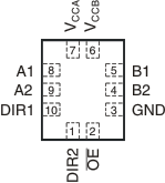
RSW PACKAGE
10-PIN UQFN
TOP VIEW

Pin Functions
| PIN | DESCRIPTION | ||
|---|---|---|---|
| NAME | NO. (UQFN) |
||
| VCCA | 7 | Supply Voltage A | |
| VCCB | 6 | Supply Voltage B | |
| GND | 3 | Ground | |
| A1 | 8 | Output or input depending on state of DIR. Output level depends on VCCA. | |
| A2 | 9 | Output or input depending on state of DIR. Output level depends on VCCA. | |
| B1 | 5 | Output or input depending on state of DIR. Output level depends on VCCB. | |
| B2 | 4 | Output or input depending on state of DIR. Output level depends on VCCB. | |
| DIR1,DIR2 | 10,1 | Direction Pin, Connect to GND or to VCCA | |
| OE | 2 | Tri-state output-mode enables. Pull OE high to place all outputs in 3-state mode. Referenced to VCCA | |