SCLS520E August 2003 – January 2015 SN74LV4051A-Q1
PRODUCTION DATA.
- 1 Features
- 2 Applications
- 3 Description
- 4 Revision History
- 5 Pin Configuration and Functions
- 6 Specifications
- 7 Parameter Measurement Information
- 8 Detailed Description
- 9 Application and Implementation
- 10Power Supply Recommendations
- 11Layout
- 12Device and Documentation Support
- 13Mechanical, Packaging, and Orderable Information
パッケージ・オプション
デバイスごとのパッケージ図は、PDF版データシートをご参照ください。
メカニカル・データ(パッケージ|ピン)
- PW|16
- DW|16
- D|16
サーマルパッド・メカニカル・データ
発注情報
1 Features
- Qualified for Automotive Applications
- AEC-Q100 Qualified With the Following Results
- Device Temperature Grade 1: –40°C to +125°C Ambient Operating Temperature Range
- Device HBM ESD Classification Level 2
- Device CDM ESD Classification Level C4B
- 2-V to 5.5-V VCC Operation
- Supports Mixed-Mode Voltage Operation on All Ports
- High On-Off Output-Voltage Ratio
- Low Crosstalk Between Switches
- Individual Switch Controls
- Extremely Low Input Current
- Latch-Up Performance Exceeds 100 mA Per JESD 78, Class II
2 Applications
- Automotive Infotainment and Cluster
- Telematics, eCall
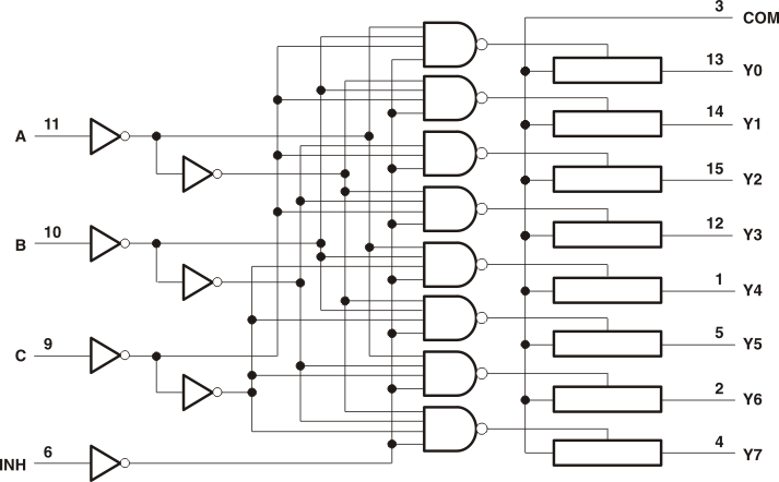
3 Description
This 8-channel CMOS analog multiplexer and demultiplexer is designed for 2-V to 5.5-V VCC operation.
The SN74LV4051A handles analog and digital signals. Each channel permits signals with amplitudes up to 5.5 V (peak) to be transmitted in either direction.
Applications include signal gating, chopping, modulation or demodulation (modem), and signal multiplexing for analog-to-digital and digital-to-analog conversion systems.
Device Information(1)
| PART NUMBER | PACKAGE | BODY SIZE (NOM) |
|---|---|---|
| SN74LV4051A-Q1 | TSSOP (16) | 5.00 mm × 4.40 mm |
| SOIC (16) | 10.30 mm × 7.50 mm | |
| 9.90 mm × 3.91 mm |
- For all available packages, see the orderable addendum at the end of the data sheet.
Logic Diagram (Positive Logic)