SCLS520E August 2003 – January 2015 SN74LV4051A-Q1
PRODUCTION DATA.
- 1 Features
- 2 Applications
- 3 Description
- 4 Revision History
- 5 Pin Configuration and Functions
- 6 Specifications
- 7 Parameter Measurement Information
- 8 Detailed Description
- 9 Application and Implementation
- 10Power Supply Recommendations
- 11Layout
- 12Device and Documentation Support
- 13Mechanical, Packaging, and Orderable Information
パッケージ・オプション
デバイスごとのパッケージ図は、PDF版データシートをご参照ください。
メカニカル・データ(パッケージ|ピン)
- PW|16
- DW|16
- D|16
サーマルパッド・メカニカル・データ
発注情報
11 Layout
11.1 Layout Guidelines
TI recommends keeping the signal lines as short and as straight as possible. Incorporation of microstrip or stripline techniques is also recommended when signal lines are more than 1 inch long. These traces must be designed with a characteristic impedance of either 50 Ω or 75 Ω,as required by the application. Do not place this device too close to high-voltage switching components, as they may cause interference.
11.2 Layout Example
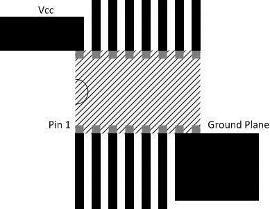 Figure 12. Layout Schematic