SCES295Z June 2000 – November 2017 SN74LVC1G06
PRODUCTION DATA.
- 1 Features
- 2 Applications
- 3 Description
- 4 Revision History
- 5 Pin Configuration and Functions
- 6 Specifications
- 7 Parameter Measurement Information
- 8 Detailed Description
- 9 Application and Implementation
- 10Power Supply Recommendations
- 11Layout
- 12Device and Documentation Support
- 13Mechanical, Packaging, and Orderable Information
パッケージ・オプション
デバイスごとのパッケージ図は、PDF版データシートをご参照ください。
メカニカル・データ(パッケージ|ピン)
- DPW|5
- DBV|5
- DSF|6
- DCK|5
- YZV|4
- DRL|5
- YZP|5
- DRY|6
サーマルパッド・メカニカル・データ
発注情報
8 Detailed Description
8.1 Overview
The SN74LVC1G06 device contains one open-drain inverter with a maximum sink current of 32 mA. This device is fully specified for partial-power-down applications using Ioff. The Ioff circuitry disables the outputs when the device is powered down. This inhibits current backflow into the device which prevents damage to the device.
8.2 Functional Block Diagram
 Figure 4. Logic Diagram (Positive Logic)
8.3 Feature Description
8.3.1 CMOS Open-Drain Outputs
The open-drain output allows the device to sink current to GND but not to source current from VCC. When the output is not actively pulling the line low, it will go into a high impedance state (tri-state). This allows the device to be used for a wide variety of applications, including up-translation and down-translation, as the output voltage can be determined by an external pullup.
The drive capability of this device creates fast edges into light loads so routing and load conditions should be considered to prevent ringing. Additionally, the outputs of this device are capable of driving larger currents than the device can sustain without being damaged. It is important for the power output of the device to be limited to avoid thermal runaway and damage due to over-current. The electrical and thermal limits defined in the Absolute Maximum Ratings must be followed at all times.
8.3.2 Standard CMOS Inputs
The impendence for standard CMOS inputs is high. Typically, a CMOS input is modeled as a resistor in parallel with the input capacitance as shown in the Electrical Characteristics. The worst case resistance is calculated with the maximum input voltage, given in the Absolute Maximum Ratings, and the maximum input leakage current, given in the Electrical Characteristics, using ohm's law (R = V ÷ I).
Signals applied to the inputs need to have fast edge rates, as defined by Δt/Δv in the Recommended Operating Conditions to avoid excessive current consumption and oscillations. If a slow or noisy input signal is required, a device with a Schmitt-trigger input should be used to condition the input signal before the standard CMOS input.
8.3.3 Negative Clamping Diodes
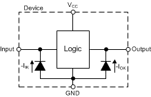
The inputs and outputs to this device have negative clamping diodes as depicted in Figure 5.
CAUTION
Voltages beyond the values specified in the Absolute Maximum Ratings table can cause damage to the device. The input negative-voltage and the output voltage ratings may be exceeded if the input and output clamp-current ratings are observed.
 Figure 5. Electrical Placement of Clamping Diodes for Each Input and Output
8.3.4 Partial Power Down (Ioff)
Each input and output enter a high impedance state when the supply voltage is 0 V. The maximum leakage into or out of any input or output pin on the device is specified by Ioff in the Electrical Characteristics.
8.3.5 Over-voltage Tolerant Inputs
Input signals to this device can be driven above the supply voltage as long as the input signals remain below the maximum input voltage value specified in the Recommended Operating Conditions.
8.4 Device Functional Modes
Table 1 lists the functional modes of the SN74LVC1G06.
Table 1. Function Table
| INPUT A |
OUTPUT Y |
|---|---|
| L | Hi-Z |
| H | L |