JAJSKA9M January 2003 – August 2022 SN74LVC1G3157
PRODUCTION DATA
- 1 特長
- 2 アプリケーション
- 3 概要
- 4 Revision History
- 5 Pin Configuration and Functions
- 6 Specifications
- 7 Parameter Measurement Information
- 8 Detailed Description
- 9 Application and Implementation
- 10Power Supply Recommendations
- 11Layout
- 12Device and Documentation Support
- 13Mechanical, Packaging, and Orderable Information
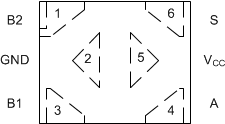
5 Pin Configuration and Functions
Figure 5-1 DBV Package,6-Pin SOT-23(Top View)
Figure 5-3 DRY Package,6-Pin SON(Top View)
Figure 5-5 DSF Package,6-Pin SON(Top View)
Figure 5-2 DCK Package,6-Pin SC70(Top View)
Figure 5-4 DRL Package,6-Pin SOT(Top View)
 Figure 5-6 DTB Package,6-Pin X2SON(Top View)
Table 5-1 Pin Functions
| PIN | TYPE(1) | DESCRIPTION | ||
|---|---|---|---|---|
| NAME | SOT-23, SC70, SON, X2SON, or SOT | |||
| B2 | 1 | I/O | Switch I/O. Set S high to enable. | |
| GND | 2 | P | Ground | |
| B1 | 3 | I/O | Switch I/O. Set S low to enable. | |
| A | 4 | I/O | Common terminal | |
| VCC | 5 | P | Power supply | |
| S | 6 | I | Select | |
(1) I = input, O = output, P = power
Figure 5-7 YZP Package,6-Pin DSBGA(Bottom View)
| Legend | |
|---|---|
| Input | Input or Output |
| Power | |
Table 5-2 Pin Functions
| PIN | TYPE(1) | DESCRIPTION | ||
|---|---|---|---|---|
| NO. | NAME | |||
| A1 | B2 | I/O | Switch I/O. Set S high to enable. | |
| A2 | S | I | Select | |
| B1 | GND | P | Ground | |
| B2 | VCC | P | Power supply | |
| C1 | B1 | I/O | Switch I/O. Set S low to enable. | |
| C2 | A | I/O | Common terminal | |
(1) I = input, O = output, P = power