SLLSE63A December 2010 – May 2016 SN75LVCP600
PRODUCTION DATA.
- 1 Features
- 2 Applications
- 3 Description
- 4 Revision History
- 5 Description (continued)
- 6 Pin Configuration and Functions
- 7 Specifications
- 8 Parameter Measurement Information
- 9 Detailed Description
- 10Application and Implementation
- 11Power Supply Recommendations
- 12Layout
- 13Device and Documentation Support
- 14Mechanical, Packaging, and Orderable Information
パッケージ・オプション
メカニカル・データ(パッケージ|ピン)
- DRF|8
サーマルパッド・メカニカル・データ
- DRF|8
発注情報
9 Detailed Description
9.1 Overview
The SN75LVCP600 is a single-channel, SATA Express, and PCIe signal conditioner supporting data rates up to
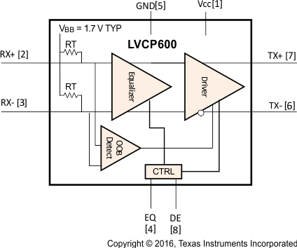
6 Gbps. The device supports SATA Gen 1, 2, and 3 specifications as well as PCIe 1, 2, and 3. The SN75LVCP600 operates from a single 3.3-V supply and has 100-Ω line termination with self-biasing feature, making the device suitable for AC coupling. The inputs incorporate an out-of-band (OOB) detector, which automatically squelches the output when the input differential voltage falls below threshold while maintaining a stable common-mode voltage. The device is also designed to handle spread spectrum clocking (SSC) transmission per SATA standard. The SN75LVCP600 handles interconnect losses at its input with selectable equalization settings that are programmable to match the loss in the channel.
For data rates of 3 Gbps and lower the SN75LVCP600 equalizes signals for a span of up to 50 inches of FR4. For data rates of 8 Gbps the device compensates up to 40 inches of FR4.
The device is hot-plug capable preventing device damage under device hot-insertion such as async signal plug or removal, unpowered plug or removal, powered plug or removal, or surprise plug or removal.
9.2 Functional Block Diagram

9.3 Feature Description
9.3.1 Input Equalization
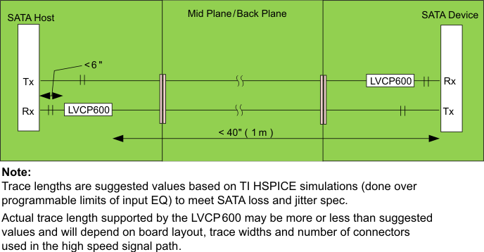
The SN75LVCP600 supports programmable equalization in its front stage; Table 1 lists the equalization settings. The input equalizer is designed to recover a signal even when no eye is present at the receiver and effectively supports FR4 trace at the input anywhere from 4" to 40" at SATA 6G speed.
Table 1. EQ and DE Settings
| EQ | EQUALIZATION (at 6 Gbps) |
DE | DE-EMPHASIS (at 6 Gbps) |
|---|---|---|---|
| 0 (default) | 7 dB | 0 (default) | 0 dB |
| 1 | 14 dB | 1 | –1.2 dB |
 Figure 9. Trace Length Example
9.3.2 Auto Low Power (ALP) Mode
Auto Low Power (ALP) Mode is triggered when a channel is in the electrical idle state for > 10 µs. The device enters and exits Low Power Mode by actively monitoring input signal (VIDpp) level. When the input signal is in the electrical idle state, that is, VIDpp < 50 mV and stays in this state for > 10 µs, the device automatically enters the low power state. In this state the output is driven to VCM and the device selectively shuts off internal circuitry to lower power by > 90% of its normal operating power. While in ALP mode the device continues actively to monitor input signal levels. When the input signal exceeds the SATA OOB upper threshold level, the device reverts to the active state. Exit time from Auto Low Power Mode is < 50 ns (maximum). See Auto Low Power.
9.3.3 Out-of-Band (OOB) Support
The squelch detector circuit within the device enables full detection of OOB signaling as specified in the SATA spec. When differential signal amplitude at the receiver input is 50 mVpp or less, the output is squelched. Differential signal amplitude of 90 mVpp or more is detected as an activity and therefore passed to the output indicating activity. Squelch circuit ON/OFF time is 5 ns (maximum). While in squelch mode outputs are held to VCM.
9.4 Device Functional Modes
9.4.1 Active
Active mode is the normal operating mode. When power is applied to the device, and the differential input signal to the receiver is greater than 90 mVpp, the device is in active mode and meets all the specifications in the data sheet.
9.4.2 Squelch
When the device is powered, and the differential input signal to the receiver is less than 50 mVpp, the device is in squelch mode. In squelch mode the transmitter outputs are both set to VCMTX or 1.7 V.
9.4.3 Auto Low Power
When the device is powered and the differential input signal to the receiver has been less than 50 mVpp for greater than 10 ns, the device transitions to Auto Low Power (ALP) mode. In ALP, the transmitter outputs are both set to VCMTX. In addition, while in ALP, the device shuts off internal circuitry to lower power to less than 10% of the power in the Active mode.