SLASET8 December 2019 TAS2110
PRODUCTION DATA.
- 1 Features
- 2 Applications
- 3 Description
- 4 Revision History
- 5 Pin Configuration and Functions
- 6 Specifications
- 7 Parameter Measurement Information
-
8 Detailed Description
- 8.1 Overview
- 8.2 Functional Block Diagram
- 8.3
Feature Description
- 8.3.1 PurePath™ Console 3 Software
- 8.3.2 Device Mode and Address Selection
- 8.3.3 General I2C Operation
- 8.3.4 Single-Byte and Multiple-Byte Transfers
- 8.3.5 Single-Byte Write
- 8.3.6 Multiple-Byte Write and Incremental Multiple-Byte Write
- 8.3.7 Single-Byte Read
- 8.3.8 Multiple-Byte Read
- 8.3.9 Register Organization
- 8.3.10 Operational Modes
- 8.3.11 Faults and Status
- 8.3.12 Power Sequencing Requirements
- 8.3.13 Digital Input Pull Downs
- 8.4
Device Functional Modes
- 8.4.1 TDM Port
- 8.4.2 Playback Signal Path
- 8.4.3 SAR ADC
- 8.4.4 Boost
- 8.4.5 Clocks and PLL
- 8.4.6 Thermal Foldback
- 8.4.7 Internal Tone Generator
- 8.5
Register Maps
- 8.5.1 Register Summary Table Page=0x00
- 8.5.2 Register Summary Table Page=0x01
- 8.5.3 Register Summary Table Page=0x02
- 8.5.4 Register Summary Table Page=0x04
- 8.5.5 PAGE0 (page=0x00 address=0x00) [reset=0h]
- 8.5.6 SW_RESET (page=0x00 address=0x01) [reset=0h]
- 8.5.7 PWR_CTL (page=0x00 address=0x02) [reset=Eh]
- 8.5.8 PB_CFG1 (page=0x00 address=0x03) [reset=20h]
- 8.5.9 MISC_CFG1 (page=0x00 address=0x04) [reset=C6h]
- 8.5.10 MISC_CFG2 (page=0x00 address=0x05) [reset=22h]
- 8.5.11 TDM_CFG0 (page=0x00 address=0x06) [reset=9h]
- 8.5.12 TDM_CFG1 (page=0x00 address=0x07) [reset=2h]
- 8.5.13 TDM_CFG2 (page=0x00 address=0x08) [reset=Ah]
- 8.5.14 TDM_CFG3 (page=0x00 address=0x09) [reset=10h]
- 8.5.15 TDM_CFG4 (page=0x00 address=0x0A) [reset=13h]
- 8.5.16 TDM_CFG7 (page=0x00 address=0x0D) [reset=4h]
- 8.5.17 TDM_CFG8 (page=0x00 address=0x0E) [reset=5h]
- 8.5.18 TDM_CFG9 (page=0x00 address=0x0F) [reset=6h]
- 8.5.19 TDM_CFG10 (page=0x00 address=0x10) [reset=7h]
- 8.5.20 TDM_DET (page=0x00 address=0x11) [reset=7Fh]
- 8.5.21 LIM_CFG_0 (page=0x00 address=0x12) [reset=12h]
- 8.5.22 LIM_CFG_1 (page=0x00 address=0x13) [reset=76h]
- 8.5.23 BOP_CFG_0 (page=0x00 address=0x14) [reset=1h]
- 8.5.24 BOP_CFG_1 (page=0x00 address=0x15) [reset=2Eh]
- 8.5.25 ICLA_CFG (page=0x00 address=0x16) [reset=60h]
- 8.5.26 GAIN_ICLA_CFG0 (page=0x00 address=0x18) [reset=Ch]
- 8.5.27 ICLA_CFG1 (page=0x00 address=0x19) [reset=0h]
- 8.5.28 INT_MASK0 (page=0x00 address=0x1A) [reset=FCh]
- 8.5.29 INT_MASK1 (page=0x00 address=0x1B) [reset=A6h]
- 8.5.30 INT_LIVE0 (page=0x00 address=0x1F) [reset=0h]
- 8.5.31 INT_LIVE1 (page=0x00 address=0x20) [reset=0h]
- 8.5.32 INT_LTCH0 (page=0x00 address=0x24) [reset=0h]
- 8.5.33 INT_LTCH1 (page=0x00 address=0x25) [reset=0h]
- 8.5.34 VBAT_MSB (page=0x00 address=0x2A) [reset=0h]
- 8.5.35 VBAT_LSB (page=0x00 address=0x2B) [reset=0h]
- 8.5.36 TEMP (page=0x00 address=0x2C) [reset=0h]
- 8.5.37 INT_CLK (page=0x00 address=0x30) [reset=19h]
- 8.5.38 DIN_PD (page=0x00 address=0x31) [reset=40h]
- 8.5.39 MISC_CFG3 (page=0x00 address=0x32) [reset=80h]
- 8.5.40 BOOST_CFG1 (page=0x00 address=0x33) [reset=34h]
- 8.5.41 BOOST_CFG2 (page=0x00 address=0x34) [reset=4Bh]
- 8.5.42 BOOST_CFG3 (page=0x00 address=0x35) [reset=74h]
- 8.5.43 MISC_CFG4 (page=0x00 address=0x3D) [reset=8h]
- 8.5.44 TG_CFG0 (page=0x00 address=0x3F) [reset=0h]
- 8.5.45 BOOST_CFG4 (page=0x00 address=0x40) [reset=36h]
- 8.5.46 REV_ID (page=0x00 address=0x7D) [reset=0h]
- 8.5.47 I2C_CKSUM (page=0x00 address=0x7E) [reset=0h]
- 8.5.48 BOOK (page=0x00 address=0x7F) [reset=0h]
- 8.5.49 PAGE1 (page=0x01 address=0x00) [reset=0h]
- 8.5.50 TF_CFG21 (page=0x01 address=0x08) [reset=40h]
- 8.5.51 PAGE2 (page=0x02 address=0x00) [reset=0h]
- 8.5.52 DVC_CFG1 (page=0x02 address=0x0C) [reset=40h]
- 8.5.53 DVC_CFG2 (page=0x02 address=0x0D) [reset=40h]
- 8.5.54 DVC_CFG3 (page=0x02 address=0x0E) [reset=0h]
- 8.5.55 DVC_CFG4 (page=0x02 address=0x0F) [reset=0h]
- 8.5.56 DVC_CFG5 (page=0x02 address=0x10) [reset=3h]
- 8.5.57 DVC_CFG6 (page=0x02 address=0x11) [reset=4Ah]
- 8.5.58 DVC_CFG7 (page=0x02 address=0x12) [reset=51h]
- 8.5.59 DVC_CFG7 (page=0x02 address=0x13) [reset=6Ch]
- 8.5.60 LIM_CFG1 (page=0x02 address=0x14) [reset=2Dh]
- 8.5.61 LIM_CFG2 (page=0x02 address=0x15) [reset=6Ah]
- 8.5.62 LIM_CFG3 (page=0x02 address=0x16) [reset=86h]
- 8.5.63 LIM_CFG4 (page=0x02 address=0x17) [reset=6Fh]
- 8.5.64 LIM_CFG5 (page=0x02 address=0x18) [reset=47h]
- 8.5.65 LIM_CFG6 (page=0x02 address=0x19) [reset=5Ch]
- 8.5.66 LIM_CFG7 (page=0x02 address=0x1A) [reset=28h]
- 8.5.67 LIM_CFG8 (page=0x02 address=0x1B) [reset=F6h]
- 8.5.68 LIM_CFG9 (page=0x02 address=0x1C) [reset=16h]
- 8.5.69 LIM_CFG10 (page=0x02 address=0x1D) [reset=66h]
- 8.5.70 LIM_CFG11 (page=0x02 address=0x1E) [reset=66h]
- 8.5.71 LIM_CFG12 (page=0x02 address=0x1F) [reset=66h]
- 8.5.72 LIM_CFG13 (page=0x02 address=0x20) [reset=34h]
- 8.5.73 LIM_CFG14 (page=0x02 address=0x21) [reset=CCh]
- 8.5.74 LIM_CFG15 (page=0x02 address=0x22) [reset=CCh]
- 8.5.75 LIM_CFG16 (page=0x02 address=0x23) [reset=CDh]
- 8.5.76 LIM_CFG17 (page=0x02 address=0x24) [reset=10h]
- 8.5.77 LIM_CFG18 (page=0x02 address=0x25) [reset=0h]
- 8.5.78 LIM_CFG19 (page=0x02 address=0x26) [reset=0h]
- 8.5.79 LIM_CFG20 (page=0x02 address=0x27) [reset=0h]
- 8.5.80 BOP_CFG1 (page=0x02 address=0x28) [reset=2Eh]
- 8.5.81 BOP_CFG2 (page=0x02 address=0x29) [reset=66h]
- 8.5.82 BOP_CFG3 (page=0x02 address=0x2A) [reset=66h]
- 8.5.83 BOP_CFG4 (page=0x02 address=0x2B) [reset=66h]
- 8.5.84 BOP_CFG5 (page=0x02 address=0x2C) [reset=2Bh]
- 8.5.85 BOP_CFG6 (page=0x02 address=0x2D) [reset=33h]
- 8.5.86 BOP_CFG7 (page=0x02 address=0x2E) [reset=33h]
- 8.5.87 BOP_CFG8 (page=0x02 address=0x2F) [reset=33h]
- 8.5.88 HPFC_CFG1 (page=0x02 address=0x30) [reset=7Fh]
- 8.5.89 HPFC_CFG2 (page=0x02 address=0x31) [reset=FBh]
- 8.5.90 HPFC_CFG3 (page=0x02 address=0x32) [reset=B6h]
- 8.5.91 HPFC_CFG4 (page=0x02 address=0x33) [reset=14h]
- 8.5.92 HPFC_CFG5 (page=0x02 address=0x34) [reset=80h]
- 8.5.93 HPFC_CFG6 (page=0x02 address=0x35) [reset=4h]
- 8.5.94 HPFC_CFG7 (page=0x02 address=0x36) [reset=49h]
- 8.5.95 HPFC_CFG8 (page=0x02 address=0x37) [reset=ECh]
- 8.5.96 HPFC_CFG9 (page=0x02 address=0x38) [reset=7Fh]
- 8.5.97 HPFC_CFG10 (page=0x02 address=0x39) [reset=7Fh]
- 8.5.98 HPFC_CFG11 (page=0x02 address=0x3A) [reset=6Ch]
- 8.5.99 HPFC_CFG12 (page=0x02 address=0x3B) [reset=28h]
- 8.5.100 TG_CFG1 (page=0x02 address=0x3C) [reset=3Fh]
- 8.5.101 TG_CFG2 (page=0x02 address=0x3D) [reset=FFh]
- 8.5.102 TG_CFG3 (page=0x02 address=0x3E) [reset=7Ah]
- 8.5.103 TG_CFG4 (page=0x02 address=0x3F) [reset=E3h]
- 8.5.104 TG_CFG5 (page=0x02 address=0x40) [reset=1h]
- 8.5.105 TG_CFG6 (page=0x02 address=0x41) [reset=1h]
- 8.5.106 TG_CFG7 (page=0x02 address=0x42) [reset=5Bh]
- 8.5.107 TG_CFG8 (page=0x02 address=0x43) [reset=4Ch]
- 8.5.108 TG_CFG9 (page=0x02 address=0x44) [reset=0h]
- 8.5.109 TG_CFG10 (page=0x02 address=0x45) [reset=0h]
- 8.5.110 TG_CFG11 (page=0x02 address=0x46) [reset=3h]
- 8.5.111 TG_CFG12 (page=0x02 address=0x47) [reset=1Fh]
- 8.5.112 TG_CFG13 (page=0x02 address=0x48) [reset=2h]
- 8.5.113 TG_CFG14 (page=0x02 address=0x49) [reset=46h]
- 8.5.114 TG_CFG15 (page=0x02 address=0x4A) [reset=B4h]
- 8.5.115 TG_CFG16 (page=0x02 address=0x4B) [reset=E4h]
- 8.5.116 TG_CFG17 (page=0x02 address=0x4C) [reset=E0h]
- 8.5.117 TG_CFG18 (page=0x02 address=0x4D) [reset=0h]
- 8.5.118 TG_CFG19 (page=0x02 address=0x4E) [reset=0h]
- 8.5.119 TG_CFG20 (page=0x02 address=0x4F) [reset=0h]
- 8.5.120 TG_CFG21 (page=0x02 address=0x50) [reset=6Eh]
- 8.5.121 TG_CFG22 (page=0x02 address=0x51) [reset=D9h]
- 8.5.122 TG_CFG23 (page=0x02 address=0x52) [reset=EBh]
- 8.5.123 TG_CFG24 (page=0x02 address=0x53) [reset=A1h]
- 8.5.124 TG_CFG25 (page=0x02 address=0x54) [reset=0h]
- 8.5.125 TG_CFG26 (page=0x02 address=0x55) [reset=0h]
- 8.5.126 TG_CFG27 (page=0x02 address=0x56) [reset=0h]
- 8.5.127 TG_CFG28 (page=0x02 address=0x57) [reset=2Ch]
- 8.5.128 TG_CFG29 (page=0x02 address=0x58) [reset=8h]
- 8.5.129 TG_CFG30 (page=0x02 address=0x59) [reset=9h]
- 8.5.130 TG_CFG31 (page=0x02 address=0x5A) [reset=BCh]
- 8.5.131 TG_CFG32 (page=0x02 address=0x5B) [reset=C4h]
- 8.5.132 LD_CFG0 (page=0x02 address=0x5C) [reset=64h]
- 8.5.133 LD_CFG1 (page=0x02 address=0x5D) [reset=0h]
- 8.5.134 LD_CFG2 (page=0x02 address=0x5E) [reset=0h]
- 8.5.135 LD_CFG3 (page=0x02 address=0x5F) [reset=0h]
- 8.5.136 LD_CFG4 (page=0x02 address=0x60) [reset=0h]
- 8.5.137 LD_CFG5 (page=0x02 address=0x61) [reset=80h]
- 8.5.138 LD_CFG6 (page=0x02 address=0x62) [reset=0h]
- 8.5.139 LD_CFG7 (page=0x02 address=0x63) [reset=0h]
- 8.5.140 IDC_CFG0 (page=0x02 address=0x64) [reset=0h]
- 8.5.141 IDC_CFG1 (page=0x02 address=0x65) [reset=20h]
- 8.5.142 IDC_CFG2 (page=0x02 address=0x66) [reset=C4h]
- 8.5.143 IDC_CFG3 (page=0x02 address=0x67) [reset=9Ch]
- 8.5.144 IDC_CFG7 (page=0x02 address=0x6C) [reset=0h]
- 8.5.145 IDC_CFG8 (page=0x02 address=0x6D) [reset=0h]
- 8.5.146 IDC_CFG9 (page=0x02 address=0x6E) [reset=12h]
- 8.5.147 IDC_CFG10 (page=0x02 address=0x6F) [reset=C0h]
- 8.5.148 TF_CFG_1 (page=0x02 address=0x7C) [reset=72h]
- 8.5.149 TF_CFG_2 (page=0x02 address=0x7D) [reset=14h]
- 8.5.150 TF_CFG_3 (page=0x02 address=0x7E) [reset=82h]
- 8.5.151 TF_CFG_4 (page=0x02 address=0x7F) [reset=C0h]
- 8.5.152 PAGE4 (page=0x04 address=0x00) [reset=0h]
- 8.5.153 LD_CFG8 (page=0x04 address=0x18) [reset=0h]
- 8.5.154 LD_CFG9 (page=0x04 address=0x19) [reset=0h]
- 8.5.155 LD_CFG10 (page=0x04 address=0x1A) [reset=0h]
- 8.5.156 LD_CFG11 (page=0x04 address=0x1B) [reset=0h]
- 8.5.157 TF_CFG4 (page=0x04 address=0x58) [reset=0h]
- 8.5.158 TF_CFG5 (page=0x04 address=0x59) [reset=0h]
- 8.5.159 TF_CFG6 (page=0x04 address=0x5A) [reset=0h]
- 8.5.160 TF_CFG7 (page=0x04 address=0x5B) [reset=64h]
- 8.5.161 TF_CFG8 (page=0x04 address=0x5C) [reset=40h]
- 8.5.162 TF_CFG9 (page=0x04 address=0x5D) [reset=BDh]
- 8.5.163 TF_CFG10 (page=0x04 address=0x5E) [reset=B7h]
- 8.5.164 TF_CFG11 (page=0x04 address=0x5F) [reset=B0h]
- 8.5.165 TF_CFG12 (page=0x04 address=0x60) [reset=39h]
- 8.5.166 TF_CFG13 (page=0x04 address=0x61) [reset=82h]
- 8.5.167 TF_CFG14 (page=0x04 address=0x62) [reset=60h]
- 8.5.168 TF_CFG16 (page=0x04 address=0x63) [reset=7Fh]
- 8.5.169 TF_CFG17 (page=0x04 address=0x64) [reset=2Dh]
- 8.5.170 TF_CFG18 (page=0x04 address=0x65) [reset=6Ah]
- 8.5.171 TF_CFG19 (page=0x04 address=0x66) [reset=86h]
- 8.5.172 TF_CFG20 (page=0x04 address=0x67) [reset=6Fh]
- 9 Application and Implementation
- 10Power Supply Recommendations
- 11Layout
- 12Device and Documentation Support
- 13Mechanical, Packaging, and Orderable Information
パッケージ・オプション
メカニカル・データ(パッケージ|ピン)
- RPP|32
サーマルパッド・メカニカル・データ
- RPP|32
発注情報
8.4.2.5 Supply Tracking Limiters with Brown Out Prevention
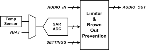
The TAS2110 monitors battery voltage (VBAT) and along with the audio signal to automatically decrease gain when the audio signal peaks exceed a programmable threshold. This helps prevent clipping and extends playback time through end of charge battery conditions. The limiters threshold can be configured to track the monitored voltage below a programmable inflection point with a programmable slope. A minimum threshold sets the limit of threshold reduction from the voltage tracking. Configurable attack rate, hold time and release rate are provided to shape the dynamic response of each limiter. If the ICLA is enabled the actual attenuation is based on the ICLA configuration using the calculated attenuation value of all devices on the selected ICLA bus.
 Figure 42. Limiter and Brown Out Prevention Interaction Diagram
 A Brown Out Prevention (BOP) feature provides a priority input to provide a fast response to transient dips in the battery supply (VBAT) which at end of charge conditions that can cause system level brown out. When the selected supply dips below the brown-out threshold the BOP will begin reducing gain at a configurable attack rate. When the VBAT supply rises above the brownout threshold, the BOP will begin to release after the programmed hold time. During a BOP event the limiter updates will be paused. This is to prevent a limiter from releasing during a BOP event. The VBAT limiter is enabled by setting the LIMB_EN bit high.
Table 47. VBAT Tracking Limiter Enable
| LIMB_EN | VALUE |
|---|---|
0
|
Disabled (default) |
1
|
Enabled |
The limiter has a configurable attack rate, hold time and release rate, which are available via the LIMB_ATK_RT[2:0], LIMB_HLD_TM[2:0], LIMB_RLS_RT[2:0] register bits. The limiter attack and release step sizes can be set by configuring the LIMB_ATK_ST[1:0] and LIMB_RLS_ST[1:0] register bits. The rates are based on the number of audio samples and actual time values can be calculated by multiplying by 1/fs. For example the attack rate of 4 samples at 48 ksps would be approximately 83 µs.
Table 48. Limiter Attack Rate
| LIMB_ATK_RT[2:0] | ATTACK RATE (samples/step) | ATTACK RATE @ 48 ksps (~µs) |
|---|---|---|
0x0
|
1 | 20 |
0x1
|
2 (default) | 42 |
0x2
|
4 | 83 |
0x3
|
8 | 167 |
0x4
|
16 | 333 |
0x5
|
32 | 666 |
0x6
|
64 | 1300 |
0x7
|
128 | 2700 |
Table 49. Limiter Hold Time
| LIMB_HLD_TM[2:0] | HOLD TIME (samples) | HOLD TIME @ 48ksps (ms) |
|---|---|---|
0x0
|
0 | 0 |
0x1
|
1920 | 40 |
0x2
|
4800 | 100 |
0x3
|
9600 | 200 |
0x4
|
19200 | 400 |
0x5
|
48000 | 1000 |
0x6
|
96000 (default) | 2000 |
0x7
|
192000 | 4000 |
Table 50. Limiter Release Rate
| LIMB_RLS_RT[2:0] | Release Rate (samples/step) | RELEASE RATE @ 48 ksps (ms) |
|---|---|---|
0x0
|
10 | 0.2 |
0x1
|
20 | 0.4 |
0x2
|
40 | 0.8 |
0x3
|
80 | 1.7 |
0x4
|
160 | 3.3 |
0x5
|
320 | 6.7 |
0x6
|
640 (default) | 13.3 |
0x7
|
1280 | 26.7 |
Table 51. Limiter Attack Step Size
| LIMB_ATK_ST[1:0] | STEP SIZE (dB) |
|---|---|
00
|
0.25 |
01
|
0.5 (default) |
10
|
1 |
11
|
2 |
Table 52. Limiter Release Step Size
| LIMB_RLS_ST[1:0] | STEP SIZE (dB) |
|---|---|
00
|
0.25 |
01
|
0.5 (default) |
10
|
1 |
11
|
2 |
A maximum level of attenuation applied by the limiters and brown out prevention feature is configurable via the LIM_MAX_ATN register. This attenuation limit is shared between the features. For instance, if the maximum attenuation is set to 6 dB and the limiters have reduced gain by 4 dB, the brown out prevention feature will only be able to reduce the gain further by another 2 dB. If the limiter or brown out prevention feature is attacking and it reaches the maximum attenuation, gain will not be reduced any further.
The limiter max attenuation LIM_MAX_ATN represent the limit in a 1.X format. To calculate the value to write to the 4 registers by apply the following formula to the desired dB using equation LIMB_MAX_ATN = round(10^(-dB/20)*2^31).
Table 53. Limiter Max Attenuation
| LIM_MAX_ATN[31:0] | ATTENUATION (dB) |
|---|---|
0x7214 82C0
|
-1 |
...
|
... |
0x2D6A 866F
|
-9 (default) |
...
|
... |
0x1326 DD71
|
-16.5 |
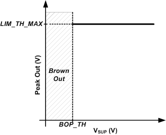
The limiter begins reducing gain when the output signal level is greater than the limiter threshold. The limiter can be configured to track selected supply below a programmable inflection point with a minimum threshold value. Figure 43 below shows the limiter configured to limit to a constant level regardless of the selected supply level. To achieve this behavior, set the limiter maximum threshold to the desired level using LIM_TH_MAX. Set the limiter inflection point using LIM_INF_PT below the minimum allowable supply setting. The limiter minimum threshold register LIM_TH_MIN does not impact limiter behavior in this use case.
 Figure 43. Limiter with Fixed Threshold
 The VBAT limiter threshold max LIMB_TH_MAX and min LIMB_TH_MIN registers represent the limit in a 5.X format. To calculate the value to write to the 4 registers by apply the following formula to the desired threshold voltage using the equation LIMB_TH_MAX or LIMB_TH_MIN = round(Volts*2^27).
Table 54. VBAT Limiter Maximum Threshold
| LIMB_TH_MAX[31:0] | THRESHOLD (V) |
|---|---|
0x1400 0000
|
2.5 |
...
|
... |
0x4800 0000
|
9 (default) |
...
|
... |
0x7C00 0000
|
15.5 |
Table 55. VBAT Limiter Minimum Threshold
| LIMB_TH_MIN[31:0] | THRESHOLD (V) |
|---|---|
0x1400 0000
|
2.5 |
...
|
... |
0x2000 0000
|
4 (default) |
...
|
... |
0x7C00 0000
|
15.5 |
The VBAT limiter inflection point LIMB_INF_PT represent the limit in a format. To calculate the value to write to the 4 registers by apply the following formula to the desired infection voltage using the equation LIMB_INF_PT = round(Volts*2^).
Table 56. VBAT Limiter Inflection Point
| LIMB_INF_PT[31:0] | THRESHOLD (V) |
|---|---|
0x2000 0000
|
2 |
...
|
... |
0x34CC CCCD
|
3.3 (default) |
...
|
... |
0x3000 0000
|
6 |
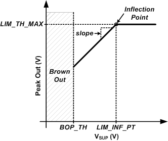
Figure 44 shows how to configure the limiter to track selected supply below a threshold without a minimum threshold. Set the LIM_TH_MAX register to the desired threshold and LIM_INF_PT register to the desired inflection point where the limiter will begin reducing the threshold with the selected supply. The default value of 1 V/V will reduce the threshold 1 V for every 1 V of drop in the supply voltage. More aggressive tracking slopes can be programmed if desired. Program the LIM_TH_MIN below the minimum the selected supply to prevent the limiter from having a minimum threshold reduction when tracking the selected supply.
The VBAT limiter tracking slope LIMB_SLOPE[31:0] represent the limit in a format. To calculate the value to write to the 4 registers by apply the following formula to the desired infection voltage using equation LIMB_SLOPE = round(slope(V/V)*2^).
 Figure 44. Limiter with Inflection Point
 Table 57. Limiter VBAT Tracking Slope
| LIMB_SLOPE[31:0] | SLOPE (V/V) |
|---|---|
0x1000 0000
|
1 (default) |
...
|
... |
0x4000 0000
|
4 |
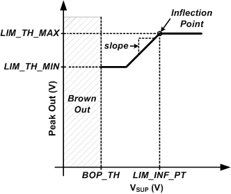
To achieve a limiter that tracks the selected supply below a threshold, configure the limiter as explained in the previous example, except program the LIM_TH_MIN register to the desired minimum threshold. This is shown in Figure 45 below.
 Figure 45. Limiter with Inflection Point and Minimum Threshold
 The TAS2110 also employs a Brown Out Prevention (BOP) feature that serves as a low latency priority input to the limiter engine that begins attacking the VBAT supply dipping below the programmed BOP threshold. This feature can be enabled by setting the BOP_EN register bit high. It should be noted that the BOP feature is independent of the limiter and will function if enabled, even if the limiter is disabled. The BOP threshold is configured by setting the threshold with register bits BOP_TH.
 Figure 46. Limiter Block Diagram
 Table 58. Brown Out Prevention Enable
| BOP_EN | VALUE |
|---|---|
0
|
Disabled |
1
|
Enabled (default) |
The Brownout prevention threshold BOP_TH represent a threshold in a 4.X format. To calculate the value to write to the 4 registers by apply the following formula to the desired brownout threshold using equation BOP_TH = round(Volts*2^28).
Table 59. Brown Out Prevention Threshold
| BOP_TH[31:0] | VBAT THRESHOLD (V) |
|---|---|
0x0000 000 - 0x1FFF FFFF
|
Reserved |
0x2000 0000
|
2.5 |
...
|
... |
0x2E66 6666
|
2.9 (default) |
...
|
... |
0x2000 0000
|
4 |
0x2000 0001 - 0xFFFF FFFF
|
Reserved |
The BOP feature has a separate attack rate BOP_ATK_RT, attack step size BOP_ATK_ST and hold time BOP_HLD_TM from the battery tracking limiter. The BOP feature uses the LIMB_RLS_RT register setting to release after a brown out event. The rates are based on the number of audio samples and actual time values can be calculated by multiplying by 1/fs. For example the attack rate of 4 samples at 48 ksps would be approximately 83 µs.
Table 60. Brown Out Prevention Attack Rate
| BOP_ATK_RT[2:0] | ATTACK RATE (samples/step) | ATTACK RATE @ 48 ksps (~µs) |
|---|---|---|
0x0
|
1 | 20 |
0x1
|
2 | 42 |
0x2
|
4 | 83 |
0x3
|
8 | 167 |
0x4
|
16 | 333 |
0x5
|
32 | 666 |
0x6
|
64 | 1300 |
0x7
|
128 | 2700 |
Table 61. Brown Out Prevention Attack Step Size
| BOP_ATK_ST[1:0] | STEP SIZE (dB) |
|---|---|
00
|
0.5 |
01
|
1 (default) |
10
|
1.5 |
11
|
2 |
Table 62. Brown Out Prevention Hold Time
| BOP_HLD_TM[2:0] | HOLD TIME (ms) |
|---|---|
0x0
|
0 |
0x1
|
10 |
0x2
|
25 |
0x3
|
50 |
0x4
|
100 |
0x5
|
250 |
0x6
|
500 (default) |
0x7
|
1000 |
The TAS2110 can also shutdown the device when a brown out event occurs if the BOP_MUTE register bit is set high. For the device to continue playing audio again, the device must transition through a SW/HW shutdown state. Setting the BOP_INF_HLD high will cause the limiter to stay in the hold state (for example never release) after a cleared brown out event until either the device transitions through a mute or SW/HW shutdown state or the register bit BOP_HLD_CLR is written to a high value (which will cause the device to exit the hold state and begin releasing). This bit is self clearing and will always readback low. Figure 47 below illustrates the entering and exiting from a brown out event.
 Figure 47. Brown Out Prevention Event
 Table 63. Shutdown on Brown Out Event
| BOP_MUTE | VALUE |
|---|---|
0
|
Don't Shutdown (default) |
1
|
Mute then shutdown |
Table 64. Infinite Hold on Brown Out Event
| BOP_INF_HLD | VALUE |
|---|---|
0
|
Use BOP_HLD_TM after Brown Out event (default) |
1
|
Do not release until BOP_HLD_CLR is asserted high |
If the TAS2110 is configured to hold the brownout event until cleared the attenuation will remain until BOP_HLD_CLR register clear is performed. This should be performed by setting the BOP_HLR_CLR bit high, reading the register and then setting the BOP_HLD_CLR back to low.
Table 65. BOP Infinite Hold Clear
| BOP_HLD_CLR | VALUE |
|---|---|
0
|
Don't clear (default) |
1
|
Clear event |
A hard brownout level can be set to shutdown the TAS2110 if the BOP cannot mitigate the drop in battery voltage VBAT. This will shutdown the device and should not be used if the BOP_MUTE is enable. The brownout shutdown will only function if brownout engine is enabled using BOP_EN.
Table 66. Brown Out Shutdown Enable
| BOSD_EN | VALUE |
|---|---|
0
|
Disabled (default) |
1
|
Enabled |
The Brownout prevention shutdown threshold BOSD_TH represent a threshold in a 5.X format. To calculate the value to write to the 4 registers by apply the following formula to the desired brownout threshold using equation BOSD_TH = round(Volts*2^27).
Table 67. Brown Out Shutdown Threshold
| BOSD_TH[31:0] | VBAT THRESHOLD (V) |
|---|---|
0x2000 0000
|
2.5 |
...
|
... |
0x2B33 3333
|
2.7 (default) |
...
|
... |
0x3FFF FFFF
|
3.99 |