JAJSGV7D April 2019 – January 2024 TAS2563
PRODUCTION DATA
- 1
- 1 特長
- 2 アプリケーション
- 3 概要
- 4 Pin Configuration and Functions
-
5 Specifications
- 5.1 Absolute Maximum Ratings
- 5.2 ESD Ratings
- 5.3 Recommended Operating Conditions
- 5.4 Thermal Information
- 5.5 Electrical Characteristics
- 5.6 I2C Timing Requirements
- 5.7 SPI Timing Requirements
- 5.8 PDM Port Timing Requirements
- 5.9 TDM Port Timing Requirements
- 5.10 Timing Diagrams
- 5.11 Typical Characteristics
- 6 Parameter Measurement Information
-
7 Detailed Description
- 7.1 Overview
- 7.2 Functional Block Diagram
- 7.3
Feature Description
- 7.3.1 PurePath Console 3 Software
- 7.3.2 Device Mode and Address Selection
- 7.3.3 General I2C Operation
- 7.3.4 General SPI Operation
- 7.3.5 Single-Byte and Multiple-Byte Transfers
- 7.3.6 Single-Byte Write
- 7.3.7 Multiple-Byte Write and Incremental Multiple-Byte Write
- 7.3.8 Single-Byte Read
- 7.3.9 Multiple-Byte Read
- 7.3.10 Register Organization
- 7.3.11 Operational Modes
- 7.3.12 Faults and Status
- 7.3.13 Digital Input Pull Downs
- 7.4 Device Functional Modes
- 7.5
Register Maps
- 7.5.1 Register Summary Table Page=0x00
- 7.5.2 PAGE (page=0x00 address=0x00) [reset=0h]
- 7.5.3 SW_RESET (page=0x00 address=0x01) [reset=0h]
- 7.5.4 PWR_CTL (page=0x00 address=0x02) [reset=Eh]
- 7.5.5 PB_CFG1 (page=0x00 address=0x03) [reset=20h]
- 7.5.6 MISC_CFG1 (page=0x00 address=0x04) [reset=C6h]
- 7.5.7 MISC_CFG2 (page=0x00 address=0x05) [reset=22h]
- 7.5.8 TDM_CFG0 (page=0x00 address=0x06) [reset=9h]
- 7.5.9 TDM_CFG1 (page=0x00 address=0x07) [reset=2h]
- 7.5.10 TDM_CFG2 (page=0x00 address=0x08) [reset=4Ah]
- 7.5.11 TDM_CFG3 (page=0x00 address=0x09) [reset=10h]
- 7.5.12 TDM_CFG4 (page=0x00 address=0x0A) [reset=13h]
- 7.5.13 TDM_CFG5 (page=0x00 address=0x0B) [reset=2h]
- 7.5.14 TDM_CFG6 (page=0x00 address=0x0C) [reset=0h]
- 7.5.15 TDM_CFG7 (page=0x00 address=0x0D) [reset=4h]
- 7.5.16 TDM_CFG8 (page=0x00 address=0x0E) [reset=5h]
- 7.5.17 TDM_CFG9 (page=0x00 address=0x0F) [reset=6h]
- 7.5.18 TDM_CFG10 (page=0x00 address=0x10) [reset=7h]
- 7.5.19 DSP Mode & TDM_DET (page=0x00 address=0x11) [reset=7Fh]
- 7.5.20 LIM_CFG0 (page=0x00 address=0x12) [reset=12h]
- 7.5.21 LIM_CFG1 (page=0x00 address=0x13) [reset=76h]
- 7.5.22 DSP FREQUENCY & BOP_CFG0 (page=0x00 address=0x14) [reset=1h]
- 7.5.23 BOP_CFG0 (page=0x00 address=0x15) [reset=2Eh]
- 7.5.24 BIL_and_ICLA_CFG0 (page=0x00 address=0x16) [reset=60h]
- 7.5.25 BIL_ICLA_CFG1 (page=0x00 address=0x17) [reset=0h]
- 7.5.26 GAIN_ICLA_CFG0 (page=0x00 address=0x18) [reset=0h]
- 7.5.27 ICLA_CFG1 (page=0x00 address=0x19) [reset=0h]
- 7.5.28 INT_MASK0 (page=0x00 address=0x1A) [reset=FCh]
- 7.5.29 INT_MASK1 (page=0x00 address=0x1B) [reset=A6h]
- 7.5.30 INT_MASK2 (page=0x00 address=0x1C) [reset=DFh]
- 7.5.31 INT_MASK3 (page=0x00 address=0x1D) [reset=FFh]
- 7.5.32 INT_LIVE0 (page=0x00 address=0x1F) [reset=0h]
- 7.5.33 INT_LIVE1 (page=0x00 address=0x20) [reset=0h]
- 7.5.34 INT_LIVE3 (page=0x00 address=0x21) [reset=0h]
- 7.5.35 INT_LIVE4 (page=0x00 address=0x22) [reset=0h]
- 7.5.36 INT_LTCH0 (page=0x00 address=0x24) [reset=0h]
- 7.5.37 INT_LTCH1 (page=0x00 address=0x25) [reset=0h]
- 7.5.38 INT_LTCH3 (page=0x00 address=0x26) [reset=0h]
- 7.5.39 INT_LTCH4 (page=0x00 address=0x27) [reset=0h]
- 7.5.40 VBAT_MSB (page=0x00 address=0x2A) [reset=0h]
- 7.5.41 VBAT_LSB (page=0x00 address=0x2B) [reset=0h]
- 7.5.42 TEMP (page=0x00 address=0x2C) [reset=0h]
- 7.5.43 INT & CLK CFG (page=0x00 address=0x30) [reset=19h]
- 7.5.44 DIN_PD (page=0x00 address=0x31) [reset=40h]
- 7.5.45 MISC (page=0x00 address=0x32) [reset=80h]
- 7.5.46 BOOST_CFG1 (page=0x00 address=0x33) [reset=34h]
- 7.5.47 BOOST_CFG2 (page=0x00 address=0x34) [reset=4Bh]
- 7.5.48 BOOST_CFG3 (page=0x00 address=0x35) [reset=74h]
- 7.5.49 MISC (page=0x00 address=0x3B) [reset=58h]
- 7.5.50 TG_CFG0 (page=0x00 address=0x3F) [reset=0h]
- 7.5.51 BST_ILIM_CFG0 (page=0x00 address=0x40) [reset=36h]
- 7.5.52 PDM_CONFIG0 (page=0x00 address=0x41) [reset=1h]
- 7.5.53 DIN_PD & PDM_CONFIG3 (page=0x00 address=0x42) [reset=F8h]
- 7.5.54 ASI2_CONFIG0 (page=0x00 address=0x43) [reset=8h]
- 7.5.55 ASI2_CONFIG1 (page=0x00 address=0x44) [reset=0h]
- 7.5.56 ASI2_CONFIG2 (page=0x00 address=0x45) [reset=1h]
- 7.5.57 ASI2_CONFIG3 (page=0x00 address=0x46) [reset=FCh]
- 7.5.58 PVDD_MSB_DSP (page=0x00 address=0x49) [reset=0h]
- 7.5.59 PVDD_LSB_DSP (page=0x00 address=0x4A) [reset=0h]
- 7.5.60 REV_ID (page=0x00 address=0x7D) [reset=0h]
- 7.5.61 I2C_CKSUM (page=0x00 address=0x7E) [reset=0h]
- 7.5.62 BOOK (page=0x00 address=0x7F) [reset=0h]
- 8 Application and Implementation
- 9 Power Supply Recommendations
- 10Layout
- 11Device and Documentation Support
- 12Revision History
- 13Mechanical, Packaging, and Orderable Information
パッケージ・オプション
デバイスごとのパッケージ図は、PDF版データシートをご参照ください。
メカニカル・データ(パッケージ|ピン)
- YBG|42
- RPP|32
サーマルパッド・メカニカル・データ
発注情報
7.3.4 General SPI Operation
The TAS2563 operates as an SPI slave over the IOVDD voltage range. To enable SPI mode the SPII2CZ_MISO pin is pulled to IOVDD using a resistor. During the device power up the pin state is queried and if high will enter SPI mode.
In the SPI control mode, the TAS2563 uses the terminals SCL_SELZ as SS, ADDR_SPICLK as SCLK, SPII2CZ_MISO as MISO, SDA_MOSI as MOSI; The SPI port allows full-duplex, synchronous, serial communication between a host processor (the master) and peripheral devices (slaves). The SPI master (in this case, the host processor) generates the synchronizing clock (driven onto SCLK) and initiates transmissions. The SPI slave device depends on a master to start and synchronize transmissions. A transmission begins when initiated by an SPI master. The byte from the SPI master begins shifting in on the slave MOSI terminal under the control of the master serial clock (driven onto SCLK). As the byte shifts in on the MOSI terminal, a byte shifts out on the MISO terminal to the master shift register.
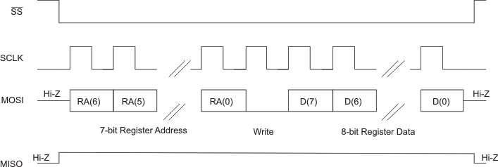
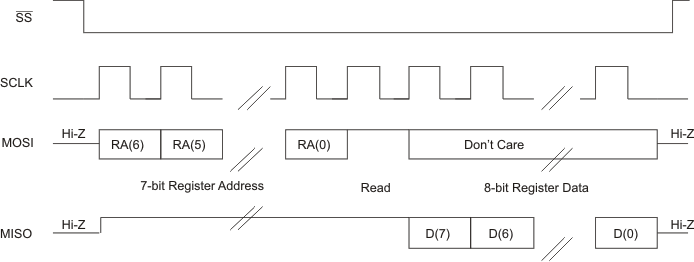
The TAS2563 interface is designed so that with a clock-phase bit setting of 1 (typical microprocessor SPI control bit CPHA = 1), the master begins driving its MOSI terminal and the slave begins driving its MISO terminal on the first serial clock edge. The SSZ terminal can remain low between transmissions; however, the TAS2563 only interprets the first 8 bits transmitted after the falling edge of SSZ as a command byte, and the next 8 bits as a data byte only if writing to a register. Reserved register bits should be written to their default values. The TAS2563 is entirely controlled by registers. Reading and writing these registers is accomplished by an 8-bit command sent to the MOSI terminal of the part prior to the data for that register. The command is structured as shown in Table 7-5 below. The first 7 bits specify the address of the register which is being written or read, from 0 to 127 (decimal). The command word ends with an R/W bit, which specifies the direction of data flow on the serial bus. In the case of a register write, the R/W bit should be set to 0. A second byte of data is sent to the MOSI terminal and contains the data to be written to the register. Reading of registers is accomplished in a similar fashion. The 8-bit command word sends the 7-bit register address, followed by the R/W bit = 1 to signify a register read is occurring. The 8-bit register data is then clocked out of the part on the MISO terminal during the second 8 SCLK clocks in the frame.
| Bit 7 | Bit 6 | Bit 5 | Bit 4 | Bit 3 | Bit 2 | Bit 1 | Bit 0 |
|---|---|---|---|---|---|---|---|
| ADDR(6) | ADDR(5) | ADDR(4) | ADDR(3) | ADDR(2) | ADDR(1) | ADDR(0) | R/WZ |
 Figure 7-4 SPI Timing Diagram for Register Write
 Figure 7-5 SPI Timing Diagram for Register Read