JAJSEN9E october 2017 – july 2023 TAS2770
PRODUCTION DATA
- 1
- 1 特長
- 2 アプリケーション
- 3 概要
- 4 Revision History
- 5 Pin Configuration and Functions
- 6 Specifications
- 7 Parameter Measurement Information
-
8 Detailed Description
- 8.1 Overview
- 8.2 Functional Block Diagram
- 8.3 Feature Description
- 8.4 Device Functional Modes
- 8.5
Register Maps
- 8.5.1 Register Summary Table Book=0x00 Page=0x00
- 8.5.2
Register Maps
- 8.5.2.1 PAGE (book=0x00 page=0x00 address=0x00) [reset=0h]
- 8.5.2.2 SW_RESET (book=0x00 page=0x00 address=0x01) [reset=0h]
- 8.5.2.3 PWR_CTL (book=0x00 page=0x00 address=0x02) [reset=Eh]
- 8.5.2.4 PB_CFG0 (book=0x00 page=0x00 address=0x03) [reset=10h]
- 8.5.2.5 PB_CFG1 (book=0x00 page=0x00 address=0x04) [reset=1h]
- 8.5.2.6 PB_CFG2 (book=0x00 page=0x00 address=0x05) [reset=0h]
- 8.5.2.7 PB_CFG3 (book=0x00 page=0x00 address=0x06) [reset=0h]
- 8.5.2.8 MISC_CFG (book=0x00 page=0x00 address=0x07) [reset=6h]
- 8.5.2.9 PDM_CFG0 (book=0x00 page=0x00 address=0x08) [reset=0h]
- 8.5.2.10 PDM_CFG1 (book=0x00 page=0x00 address=0x09) [reset=8h]
- 8.5.2.11 TDM_CFG0 (book=0x00 page=0x00 address=0x0A) [reset=7h]
- 8.5.2.12 TDM_CFG1 (book=0x00 page=0x00 address=0x0B) [reset=2h]
- 8.5.2.13 TDM_CFG2 (book=0x00 page=0x00 address=0x0C) [reset=Ah]
- 8.5.2.14 TDM_CFG3 (book=0x00 page=0x00 address=0x0D) [reset=10h]
- 8.5.2.15 TDM_CFG4 (book=0x00 page=0x00 address=0x0E) [reset=13h]
- 8.5.2.16 TDM_CFG5 (book=0x00 page=0x00 address=0x0F) [reset=2h]
- 8.5.2.17 TDM_CFG6 (book=0x00 page=0x00 address=0x10) [reset=0h]
- 8.5.2.18 TDM_CFG7 (book=0x00 page=0x00 address=0x11) [reset=4h]
- 8.5.2.19 TDM_CFG8 (book=0x00 page=0x00 address=0x12) [reset=6h]
- 8.5.2.20 TDM_CFG9 (book=0x00 page=0x00 address=0x13) [reset=7h]
- 8.5.2.21 TDM_CFG10 (book=0x00 page=0x00 address=0x14) [reset=8h]
- 8.5.2.22 LIM_CFG0 (book=0x00 page=0x00 address=0x15) [reset=14h]
- 8.5.2.23 LIM_CFG1 (book=0x00 page=0x00 address=0x16) [reset=76h]
- 8.5.2.24 LIM_CFG2 (book=0x00 page=0x00 address=0x17) [reset=10h]
- 8.5.2.25 LIM_CFG3 (book=0x00 page=0x00 address=0x18) [reset=6Eh]
- 8.5.2.26 LIM_CFG4 (book=0x00 page=0x00 address=0x19) [reset=1Eh]
- 8.5.2.27 LIM_CFG5 (book=0x00 page=0x00 address=0x1A) [reset=58h]
- 8.5.2.28 BOP_CFG0 (book=0x00 page=0x00 address=0x1B) [reset=1h]
- 8.5.2.29 BOP_CFG1 (book=0x00 page=0x00 address=0x1C) [reset=14h]
- 8.5.2.30 BOP_CFG2 (book=0x00 page=0x00 address=0x1D) [reset=4Eh]
- 8.5.2.31 ICLA_CFG0 (book=0x00 page=0x00 address=0x1E) [reset=0h]
- 8.5.2.32 ICLA_CFG1 (book=0x00 page=0x00 address=0x1F) [reset=0h]
- 8.5.2.33 INT_MASK0 (book=0x00 page=0x00 address=0x20) [reset=FCh]
- 8.5.2.34 INT_MASK1 (book=0x00 page=0x00 address=0x21) [reset=B1h]
- 8.5.2.35 INT_LIVE0 (book=0x00 page=0x00 address=0x22) [reset=0h]
- 8.5.2.36 INT_LIVE1 (book=0x00 page=0x00 address=0x23) [reset=0h]
- 8.5.2.37 INT_LTCH0 (book=0x00 page=0x00 address=0x24) [reset=0h]
- 8.5.2.38 INT_LTCH1 (book=0x00 page=0x00 address=0x25) [reset=0h]
- 8.5.2.39 INT_LTCH2 (book=0x00 page=0x00 address=0x26) [reset=0h]
- 8.5.2.40 VBAT_MSB (book=0x00 page=0x00 address=0x27) [reset=0h]
- 8.5.2.41 VBAT_LSB (book=0x00 page=0x00 address=0x28) [reset=0h]
- 8.5.2.42 TEMP_MSB (book=0x00 page=0x00 address=0x29) [reset=0h]
- 8.5.2.43 TEMP_LSB (book=0x00 page=0x00 address=0x2A) [reset=0h]
- 8.5.2.44 INT_CFG (book=0x00 page=0x00 address=0x30) [reset=5h]
- 8.5.2.45 DIN_PD (book=0x00 page=0x00 address=0x31) [reset=0h]
- 8.5.2.46 MISC_IRQ (book=0x00 page=0x00 address=0x32) [reset=81h]
- 8.5.2.47 CLOCK_CFG (book=0x00 page=0x00 address=0x3C) [reset=Dh]
- 8.5.2.48 TDM_DET (book=0x00 page=0x00 address=0x77) [reset=7Fh]
- 8.5.2.49 REV_ID (book=0x00 page=0x00 address=0x7D) [reset=20h]
- 8.5.2.50 I2C_CKSUM (book=0x00 page=0x00 address=0x7E) [reset=0h]
- 8.5.2.51 BOOK (book=0x00 page=0x00 address=0x7F) [reset=0h]
-
9 Application and Implementation
- 9.1 Application Information
- 9.2 Typical Application
- 9.3
Initialization Set Up
- 9.3.1 Initial Device Configuration - Auto Rate
- 9.3.2 Initial Device Configuration - 48 kHz
- 9.3.3 Initial Device Configuration - 44.1 kHz
- 9.3.4 Sample Rate Change - 48 kHz to 44.1kHz
- 9.3.5 Sample Rate Change - 44.1 kHz to 48 kHz
- 9.3.6 Device Mute
- 9.3.7 Device Un-Mute
- 9.3.8 Device Sleep
- 9.3.9 Device Wake
- 10Power Supply Recommendations
- 11Layout
- 12Device and Documentation Support
- 13Mechanical, Packaging, and Orderable Information
パッケージ・オプション
メカニカル・データ(パッケージ|ピン)
サーマルパッド・メカニカル・データ
発注情報
8.4.3.2 Digital Volume Control and Amplifier Output Level
The gain from audio input to speaker terminals is controlled by setting the amplifier’s output level and digital volume control (DVC). A separate DVC is provided for PDM (available from the PDM input pins) and PCM (available from the TDM ports pins) playback paths.
Amplifier output level settings are presented in dBV (dB relative to 1 Vrms) with a full scale digital audio input (0 dBFS) and the digital volume control set to 0 dB. It should be noted that these levels may not be achievable because of analog clipping in the amplifier, so they should be used to convey gain only. Table 8-37 below shows analog gain settings that can be programmed via the AMP_LEVEL[4:0] register bits.
| AMP_LEVEL[4:0] | FULL SCALE OUTPUT | |
|---|---|---|
| dBV | VPEAK (V) | |
| 11.0 | 5.02 |
| 11.5 | 5.32 |
| 12.0 | 5.63 |
| 12.5 | 5.96 |
| 13.0 | 6.32 |
| 13.5 | 6.69 |
| 14.0 | 7.09 |
| 14.5 | 7.51 |
| 15.0 | 7.95 |
| 15.5 | 8.42 |
| 16.0 | 8.92 |
| 16.5 | 9.45 |
| 17.0 | 10.0 |
| 17.5 | 10.6 |
| 18.0 | 11.2 |
| 18.5 | 11.9 |
| 19.0 (default) | 12.6 (default) |
| 19.5 | 13.4 |
| 20.0 | 14.1 |
| 20.5 | 14.98 |
| 21.0 | 15.87 |
| Reserved | Reserved |
Equation 1 calculates the amplifiers output voltage.

where
- VAMP is the amplifier output voltage in dBV
- Input is the digital input amplitude in dB with respect to 0 dBFS
- Advc is the digital volume control setting, 0 dB to -100 dB in 0.5 dB steps
- AAMP is the amplifier output level setting in dBV
The digital volume control (DVC) is independently configurable for PCM and PDM streams from 0 dB to -100 dB in 0.5 dB steps by setting the DVC_PCM[7:0] and PVC_PDM[7:0] register bits respectively. Settings greater than 0xC8 are interpreted as mute. When a change in digital volume control occurs, the device ramps the volume to the new setting based on the DVC_RATE[1:0] register bits. If DVC_RATE[1:0] is set to 2'b11, volume ramping is disabled. This can be used to speed up startup, shutdown and digital volume changes when volume ramping is handled by the system master.
| DVC_PCM[7:0] | Volume (dB) |
|---|---|
| 0 (default) |
| -0.5 |
| -1 |
| ... |
| -100 |
| Mute |
| DVC_PDM[7:0] | Volume (dB) |
|---|---|
| 0 (default) |
| -0.5 |
| -1 |
| ... |
| -100 |
| Mute |
| DVC_RAMP[1:0] | Ramp Rate |
|---|---|
| 0.5 dB per 1 Sample (default) |
| 0.5 dB per 4 Samples |
| 0.5 dB per 8 Samples |
| Volume Ramping Disabled |
The Class-D amplifier uses a closed-loop architecture, so the gain does not depend on VBAT. The approximate threshold for the onset of analog clipping is calculated in Equation 2.
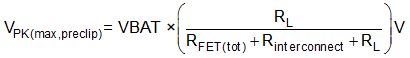
where
- VPK(max,preclip) is the maximum peak unclipped output voltage in V
- VBAT is the power supply voltage
- RL is the speaker load in Ω
- Rinterconnect is the additional resistance in the PCB (such as cabling and filters) in Ω
- RFET(on) is the power stage total on resistance (HS FET+LS FET+Sense Resistor+bonding+packaging) in Ω
The effective on-resistance for this device (including HS+LS FET, Sense Resistor and bonding and packaging leads) is approximately 510 mΩ at room temperature. Table 8-41 shows approximate maximum unclipped peak output voltages at room temperature (excluding interconnect resistances).
| SUPPLY VOLTAGE VBAT (V) | MAXIMUM UNCLIPPED PEAK VOLTAGE VPK (V) | |
|---|---|---|
| RL = 4 Ω | RL = 8 Ω | |
| 8.4 | 7.45 | 7.90 |
| 12.6 | 11.18 | 11.84 |