JAJSN80E August 2009 – May 2022 TCA9535
PRODUCTION DATA
- 1 特長
- 2 アプリケーション
- 3 概要
- 4 Revision History
- 5 Pin Configuration and Functions
- 6 Specifications
- 7 Detailed Description
- 8 Application and Implementation
- 9 Power Supply Recommendations
- 10Layout
- 11Device and Documentation Support
- 12Mechanical, Packaging, and Orderable Information
パッケージ・オプション
メカニカル・データ(パッケージ|ピン)
サーマルパッド・メカニカル・データ
発注情報
7.5.1.1.1 Writes
To write on the I2C bus, the controller sends a START condition on the bus with the address of the target, as well as the last bit (the R/ W bit) set to 0, which signifies a write. After the target sends the acknowledge bit, the controller then sends the register address of the register to which it wishes to write. The target acknowledges again, letting the controller know it is ready. After this, the controller starts sending the register data to the target until the controller has sent all the data necessary (which is sometimes only a single byte), and the controller terminates the transmission with a STOP condition.
See the Control Register and Command Byte section to see list of the TCA9535 internal registers and a description of each one.
Figure 7-5 shows an example of writing a single byte to a target register.
 Figure 7-5 Write to
Register
Figure 7-5 Write to
RegisterFigure 7-6 shows the Write to the Polarity Inversion Register.
 Figure 7-6 Write to the Polarity Inversion Register
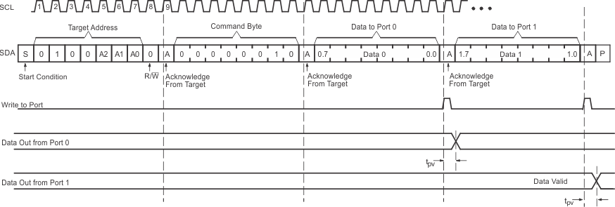
Figure 7-7 shows the Write to Output Port Registers.
 Figure 7-7 Write to Output Port Registers