JAJSH42D February 2016 – October 2021 TCAN1042-Q1 , TCAN1042G-Q1 , TCAN1042GV-Q1 , TCAN1042H-Q1 , TCAN1042HG-Q1 , TCAN1042HGV-Q1 , TCAN1042HV-Q1 , TCAN1042V-Q1
PRODUCTION DATA
- 1 特長
- 2 アプリケーション
- 3 概要
- 4 Revision History
- 5 Device Comparison Table
- 6 Pin Configurations and Functions
- 7 Specifications
- 8 Parameter Measurement Information
-
9 Detailed Description
- 9.1 Overview
- 9.2 Functional Block Diagram
- 9.3 Feature Description
- 9.4 Device Functional Modes
- 10Application Information Disclaimer
- 11Power Supply Recommendations
- 12Device and Documentation Support
- 13Mechanical, Packaging, and Orderable Information
パッケージ・オプション
デバイスごとのパッケージ図は、PDF版データシートをご参照ください。
メカニカル・データ(パッケージ|ピン)
- D|8
- DRB|8
サーマルパッド・メカニカル・データ
発注情報
9.3.1 TXD Dominant Timeout (DTO)
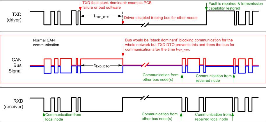
During normal mode (the only mode where the CAN driver is active), the TXD DTO circuit prevents the transceiver from blocking network communication in the event of a hardware or software failure where TXD is held dominant longer than the timeout period tTXD_DTO. The DTO circuit timer starts on a falling edge on TXD. The DTO circuit disables the CAN bus driver if no rising edge is seen before the timeout period expires. This frees the bus for communication between other nodes on the network. The CAN driver is re-activated when a recessive signal is seen on the TXD terminal, thus clearing the TXD DTO condition. The receiver and RXD terminal still reflect activity on the CAN bus, and the bus terminals are biased to the recessive level during a TXD dominant timeout.
 Figure 9-1 Example Timing Diagram for TXD DTO
The minimum dominant TXD time allowed by the TXD DTO circuit limits the minimum possible transmitted data rate of the device. The CAN protocol allows a maximum of eleven successive dominant bits (on TXD) for the worst case, where five successive dominant bits are followed immediately by an error frame. This, along with the tTXD_DTO minimum, limits the minimum data rate. Calculate the minimum transmitted data rate by: Minimum Data Rate = 11 / tTXD_DTO.