JAJSL64D April   2016  – June 2021 THS4551

PRODUCTION DATA  

  1. 特長
  2. アプリケーション
  3. 概要
  4. Revision History
  5. Companion Devices
  6. Pin Configuration and Functions
  7. Specifications
    1. 7.1 Absolute Maximum Ratings
    2. 7.2 ESD Ratings
    3. 7.3 Recommended Operating Conditions
    4. 7.4 Thermal Information
    5. 7.5 Electrical Characteristics: (VS+) – (VS–) = 5 V
    6. 7.6 Electrical Characteristics: (VS+) – (VS–) = 3 V
    7. 7.7 Typical Characteristics: (VS+) – (VS–) = 5 V
    8. 7.8 Typical Characteristics: (VS+) – (VS–) = 3 V
    9. 7.9 Typical Characteristics: 3-V to 5-V Supply Range
  8. Parameter Measurement Information
    1. 8.1 Example Characterization Circuits
    2. 8.2 Output Interface Circuit for DC-Coupled Differential Testing
    3. 8.3 Output Common-Mode Measurements
    4. 8.4 Differential Amplifier Noise Measurements
    5. 8.5 Balanced Split-Supply Versus Single-Supply Characterization
    6. 8.6 Simulated Characterization Curves
    7. 8.7 Terminology and Application Assumptions
  9. Detailed Description
    1. 9.1 Overview
    2. 9.2 Functional Block Diagram
    3. 9.3 Feature Description
      1. 9.3.1 Differential Open-Loop Gain and Output Impedance
      2. 9.3.2 Setting Resistor Values Versus Gain
      3. 9.3.3 I/O Headroom Considerations
      4. 9.3.4 Output DC Error and Drift Calculations and the Effect of Resistor Imbalances
    4. 9.4 Device Functional Modes
      1. 9.4.1 Operation from Single-Ended Sources to Differential Outputs
        1. 9.4.1.1 AC-Coupled Signal Path Considerations for Single-Ended Input to Differential Output Conversions
        2. 9.4.1.2 DC-Coupled Input Signal Path Considerations for Single-Ended to Differential Conversions
      2. 9.4.2 Operation from a Differential Input to a Differential Output
        1. 9.4.2.1 AC-Coupled, Differential-Input to Differential-Output Design Issues
        2. 9.4.2.2 DC-Coupled, Differential-Input to Differential-Output Design Issues
      3. 9.4.3 Input Overdrive Performance
  10. 10Application and Implementation
    1. 10.1 Application Information
      1. 10.1.1 Noise Analysis
      2. 10.1.2 Factors Influencing Harmonic Distortion
      3. 10.1.3 Driving Capacitive Loads
      4. 10.1.4 Interfacing to High-Performance Precision ADCs
      5. 10.1.5 Operating the Power Shutdown Feature
      6. 10.1.6 Designing Attenuators
      7. 10.1.7 The Effect of Adding a Feedback Capacitor
    2. 10.2 Typical Applications
      1. 10.2.1 An MFB Filter Driving an ADC Application
        1. 10.2.1.1 Design Requirements
        2. 10.2.1.2 Detailed Design Procedure
        3. 10.2.1.3 Application Curves
      2. 10.2.2 Differential Transimpedance Output to a High-Grade Audio PCM DAC Application
        1. 10.2.2.1 Design Requirements
        2. 10.2.2.2 Detailed Design Procedure
        3. 10.2.2.3 Application Curves
      3. 10.2.3 ADC3k Driver with a 2nd-Order RLC Interstage Filter Application
        1. 10.2.3.1 Design Requirements
        2. 10.2.3.2 Detailed Design Procedure
        3. 10.2.3.3 Application Curve
  11. 11Power Supply Recommendations
    1. 11.1 Thermal Analysis
  12. 12Layout
    1. 12.1 Layout Guidelines
      1. 12.1.1 Board Layout Recommendations
    2. 12.2 Layout Example
    3. 12.3 EVM Board
  13. 13Device and Documentation Support
    1. 13.1 Device Support
      1. 13.1.1 TINA-TI Simulation Model Features
    2. 13.2 Documentation Support
      1. 13.2.1 Related Documentation
    3. 13.3 Receiving Notification of Documentation Updates
    4. 13.4 サポート・リソース
    5. 13.5 Trademarks
    6. 13.6 Electrostatic Discharge Caution
    7. 13.7 Glossary
  14. 14Mechanical, Packaging, and Orderable Information

パッケージ・オプション

メカニカル・データ(パッケージ|ピン)
サーマルパッド・メカニカル・データ
発注情報

Application Curves

Probing the response to the output pins by using the THS4551 SBOC471 TINA-TI™ simulation model (before the RC filter to the SAR ADC) illustrates the expected response plus some peaking at higher frequencies. Any signal or noise peaking that appears at the output because of this peaking is rolled off by the RC filter between the FDA and SAR inputs. A place for a differential input capacitor is illustrated in Figure 10-11 (as 0.1 pF) but is not used for this simulation. This slight peaking is a combination of low phase margin and feedthrough via the feedback capacitor to the increasing open-loop output impedance of Figure 9-3. The loop gain and phase response are available as a TINA-TI™ simulation file.

Obtaining the SNR to the ADC input pins, and assuming an 8-VPP full scale (2.83 VRMS), gives the result of Figure 10-13. The 113-dB SNR shown in Figure 10-13 does not limit the performance for any SAR application.
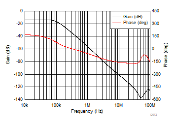
GUID-BF4F281D-DFED-4E48-9001-ACEF1D5F12CB-low.gifFigure 10-12 Gain and Phase Plot for a 100-kHz Butterworth Filter
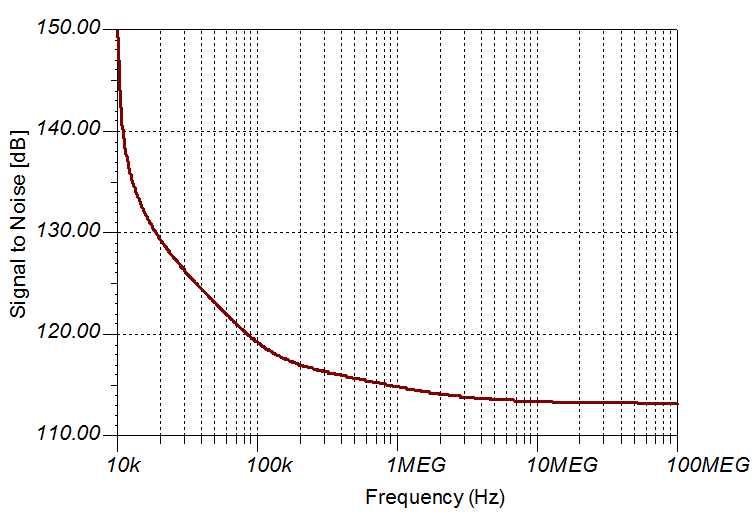
GUID-AF4C2457-4D91-4E96-B316-FB3C1D63A7E0-low.gifFigure 10-13 Signal-to-Noise Ratio Plot