JAJSIB3D August 2017 – February 2021 THS4561
PRODUCTION DATA
- 1 特長
- 2 アプリケーション
- 3 概要
- 4 Revision History
- 5 Device Comparison Table
- 6 Pin Configuration and Functions
-
7 Specifications
- 7.1 Absolute Maximum Ratings
- 7.2 ESD Ratings
- 7.3 Recommended Operating Conditions
- 7.4 Thermal Information
- 7.5 Electrical Characteristics: VS+ – VS– = 5 V to 12 V
- 7.6 Typical Characteristics: (VS+) – (VS–) = 12 V
- 7.7 Typical Characteristics: (VS+) – (VS–) = 5 V
- 7.8 Typical Characteristics: (VS+) – (VS–) = 3 V
- 7.9 Typical Characteristics: (VS+) – (VS–) = 3-V to 12-V Supply Range
-
8 Parameter Measurement Information
- 8.1 Example Characterization Circuits
- 8.2 Output Interface Circuit for DC-Coupled Differential Testing
- 8.3 Output Common-Mode Measurements
- 8.4 Differential Amplifier Noise Measurements
- 8.5 Balanced Split-Supply Versus Single-Supply Characterization
- 8.6 Simulated Characterization Curves
- 8.7 Terminology and Application Assumptions
- 9 Detailed Description
- 10Application and Implementation
- 11Power Supply Recommendations
- 12Layout
- 13Device and Documentation Support
- 14Mechanical, Packaging, and Orderable Information
パッケージ・オプション
メカニカル・データ(パッケージ|ピン)
サーマルパッド・メカニカル・データ
発注情報
9.4.3.1 AC-Coupled, Differential-Input to Differential-Output Design Issues
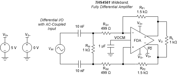
The most common way to use the THS4561 with an AC-coupled differential source is to simply couple the input into the RG resistors through the blocking capacitors. Figure 9-1 shows a typical blocking capacitor approach to a differential input. An optional input differential termination resistor (RM) is included in this design. The RM element allows the input RG resistors to be scaled up and still delivers lower differential input impedance to the source. In this example, the RG elements sum to show a 1-kΩ differential impedance and the RM element combines in parallel to provide a net 500-Ω ac differential impedance to the source. Again, the design ideally proceeds by selecting the RF element values, then the RG to set the differential gain, and then an RM element (if needed) to achieve a target input impedance. Alternatively, the RM element can be eliminated, with the 2 × RG elements set to the desired input impedance and RF set to obtain the differential gain (equal to RF / RG).
 Figure 9-1 Example AC-Coupled Differential Input Design
The DC biasing for an AC-coupled differential input design is very simple. The output VOCM is set by the VOCM input control voltage and, because there is no DC current path for the output common-mode voltage (as long as RM is only differential and not split and connected to ground for instance), the VOCM DC bias also sets the common-mode operating points for the input pins. For a purely differential input, the voltages on the input pins remain fixed at the output VOCM setting and do not move with the input signal (unlike the single-ended input configurations where the input pin common-mode voltages do move with the input signal).