JAJSIB3D August 2017 – February 2021 THS4561
PRODUCTION DATA
- 1 特長
- 2 アプリケーション
- 3 概要
- 4 Revision History
- 5 Device Comparison Table
- 6 Pin Configuration and Functions
-
7 Specifications
- 7.1 Absolute Maximum Ratings
- 7.2 ESD Ratings
- 7.3 Recommended Operating Conditions
- 7.4 Thermal Information
- 7.5 Electrical Characteristics: VS+ – VS– = 5 V to 12 V
- 7.6 Typical Characteristics: (VS+) – (VS–) = 12 V
- 7.7 Typical Characteristics: (VS+) – (VS–) = 5 V
- 7.8 Typical Characteristics: (VS+) – (VS–) = 3 V
- 7.9 Typical Characteristics: (VS+) – (VS–) = 3-V to 12-V Supply Range
-
8 Parameter Measurement Information
- 8.1 Example Characterization Circuits
- 8.2 Output Interface Circuit for DC-Coupled Differential Testing
- 8.3 Output Common-Mode Measurements
- 8.4 Differential Amplifier Noise Measurements
- 8.5 Balanced Split-Supply Versus Single-Supply Characterization
- 8.6 Simulated Characterization Curves
- 8.7 Terminology and Application Assumptions
- 9 Detailed Description
- 10Application and Implementation
- 11Power Supply Recommendations
- 12Layout
- 13Device and Documentation Support
- 14Mechanical, Packaging, and Orderable Information
パッケージ・オプション
メカニカル・データ(パッケージ|ピン)
サーマルパッド・メカニカル・データ
発注情報
10.1.3 Noise Analysis
The first step in the output noise analysis is to reduce the application circuit to the simplest form with equal feedback and gain setting elements to ground. Figure 10-4 shows the simplest analysis circuit with the FDA and resistor noise terms to be considered.
 Figure 10-4 FDA Noise Analysis Circuit
The noise powers are shown in Figure 10-4 for each term. When the RF and RG terms are matched on each side, the total differential output noise is the root sum squared (RSS) of these separate terms. Using NG ≡ 1 + RF / RG, the total output noise is given by Equation 5. Each resistor noise term is a 4kT × R power (4kT = 1.6E-20J at 290K).
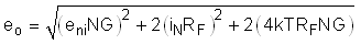
The first term is simply the differential input spot noise times the noise gain, the second term is the input current noise terms times the feedback resistor (and because there are two uncorrelated current noise terms, the power is two times one of them), and the last term is the output noise resulting from both the RF and RG resistors, at again twice the value for the output noise power of each side added together. Running a wide sweep of gains when holding RF close to 1.5 kΩ and setting the input up for a 50-Ω match gives the standard values and resulting noise listed in Table 10-2.
When the gain increases, the input-referred noise approaches only the gain of the FDA input voltage noise term at 5 nV/√ Hz.
| GAIN (V/V) | RF | RG1 | RT | RG2 | ZIN | AV | eO (nV/√ Hz) | eI (nV/√ Hz) |
|---|---|---|---|---|---|---|---|---|
| 0.1 | 1500 | 15000 | 49.9 | 15000 | 49.74 | 0.09973 | 9.15 | 91.53 |
| 1 | 1500 | 1500 | 51.1 | 1500 | 49.82 | 0.994 | 14.03 | 14.03 |
| 2 | 1500 | 750 | 52.3 | 768 | 49.98 | 1.978 | 18.99 | 9.49 |
| 5 | 1500 | 287 | 54.9 | 316 | 49.6 | 5.014 | 33.20 | 6.64 |
| 10 | 1500 | 137 | 61.9 | 165 | 50.4 | 10.08 | 55.05 | 5.51 |