JAJSDR6C August 2017 – February 2022 TIC12400-Q1
PRODUCTION DATA
- 1 特長
- 2 アプリケーション
- 3 概要
- 4 Revision History
- 5 Pin Configuration and Functions
- 6 Specifications
- 7 Parameter Measurement Information
-
8 Detailed Description
- 8.1 Overview
- 8.2 Functional Block Diagram
- 8.3
Feature Description
- 8.3.1 VS Pin
- 8.3.2 VDD Pin
- 8.3.3 Device Initialization
- 8.3.4 Device Trigger
- 8.3.5 Device Reset
- 8.3.6 VS Under-Voltage (UV) Condition
- 8.3.7 VS Over-Voltage (OV) Condition
- 8.3.8 Switch Inputs Settings
- 8.3.9 Interrupt Generation and INT Assertion
- 8.3.10 Temperature Monitor
- 8.3.11 Parity Check and Parity Generation
- 8.3.12 Cyclic Redundancy Check (CRC)
- 8.4 Device Functional Modes
- 8.5 Programming
- 8.6 Register Maps
- 8.7 Programming Guidelines
- 9 Application Information Disclaimer
- 10Power Supply Recommendations
- 11Layout
- 12Device and Documentation Support
- 13Mechanical, Packaging, and Orderable Information
パッケージ・オプション
メカニカル・データ(パッケージ|ピン)
- DCP|38
サーマルパッド・メカニカル・データ
- DCP|38
発注情報
8.4.1 Continuous Mode
In continuous mode, wetting current is continuously applied to each enabled input channel, and the status of each channel is sampled sequentially (starting from the IN0 to IN23). The TIC12400-Q1 monitors enabled inputs and issues an interrupt (if enabled) if a switch status change event is detected. The wetting current setting for each input can be individually adjusted by configuring the WC_CFG0 and WC_CFG1 to the 0 mA, 1 mA, 2 mA, 5 mA, 10 mA, or 15 mA setting. Each input is monitored by either a comparator or an ADC depending on the setting of the input mode in the register MODE.
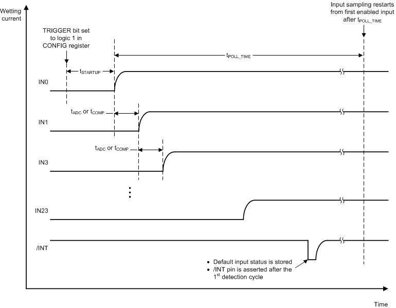
Figure 8-11 below illustrates an example of the timing diagram of the detection sequence in continuous mode. After the TRIGGER bit in register CONFIG is set to logic 1, it takes tSTARTUP to activate the wetting current for all enabled inputs. The wetting currents stay on continuously, while each input is routed to the ADC and comparator for sampling in a sequential fashion. After conversion and comparison is done for an input, the switch status (below or above detection threshold) is stored in registers (IN_STAT_COMP for comparator inputs and IN_STAT_ADC0 to IN_STAT_ADC1 for ADC inputs) to be used as the default state for subsequent detection cycles. The digital values (if the input is configured as ADC input mode) are stored in the registers ANA_STAT0 to ANA_STAT11. After the end of the first polling cycle, the INT pin is asserted low to notify the microcontroller that the default switch status is ready to be read. The SSC bit in INT_STAT register and the SPI status flag SSC are also asserted to logic 1. The polling cycle time (tPOLL) determines how frequently each input is sampled and can be configured in the register CONFIG.
 Figure 8-11 An Example of the Detection Sequence in Continuous Mode
The INT_STAT register is cleared and INT pin de-asserted if a SPI READ command is issued to the register. Note: the interrupt is always generated after the 1st detection cycle (after the TRIGGER bit in register CONFIG is set to logic 1). In subsequent detection cycles, the interrupt is generated only if switch status change is detected.
No wetting currents are applied to 0 mA- configured inputs, although some biasing current (as specified by IIN_LEAK_0mA) may still flow in and out of the input. Threshold crossing monitoring is still performed for the input using one or more of the defined thresholds. The 0 mA setting is useful for the integrated ADC or comparator to measure applied voltage on a specific input without being affected by the device wetting current.