JAJSDR6C August 2017 – February 2022 TIC12400-Q1
PRODUCTION DATA
- 1 特長
- 2 アプリケーション
- 3 概要
- 4 Revision History
- 5 Pin Configuration and Functions
- 6 Specifications
- 7 Parameter Measurement Information
-
8 Detailed Description
- 8.1 Overview
- 8.2 Functional Block Diagram
- 8.3
Feature Description
- 8.3.1 VS Pin
- 8.3.2 VDD Pin
- 8.3.3 Device Initialization
- 8.3.4 Device Trigger
- 8.3.5 Device Reset
- 8.3.6 VS Under-Voltage (UV) Condition
- 8.3.7 VS Over-Voltage (OV) Condition
- 8.3.8 Switch Inputs Settings
- 8.3.9 Interrupt Generation and INT Assertion
- 8.3.10 Temperature Monitor
- 8.3.11 Parity Check and Parity Generation
- 8.3.12 Cyclic Redundancy Check (CRC)
- 8.4 Device Functional Modes
- 8.5 Programming
- 8.6 Register Maps
- 8.7 Programming Guidelines
- 9 Application Information Disclaimer
- 10Power Supply Recommendations
- 11Layout
- 12Device and Documentation Support
- 13Mechanical, Packaging, and Orderable Information
パッケージ・オプション
メカニカル・データ(パッケージ|ピン)
- DCP|38
サーマルパッド・メカニカル・データ
- DCP|38
発注情報
8.4.2.2 Matrix polling
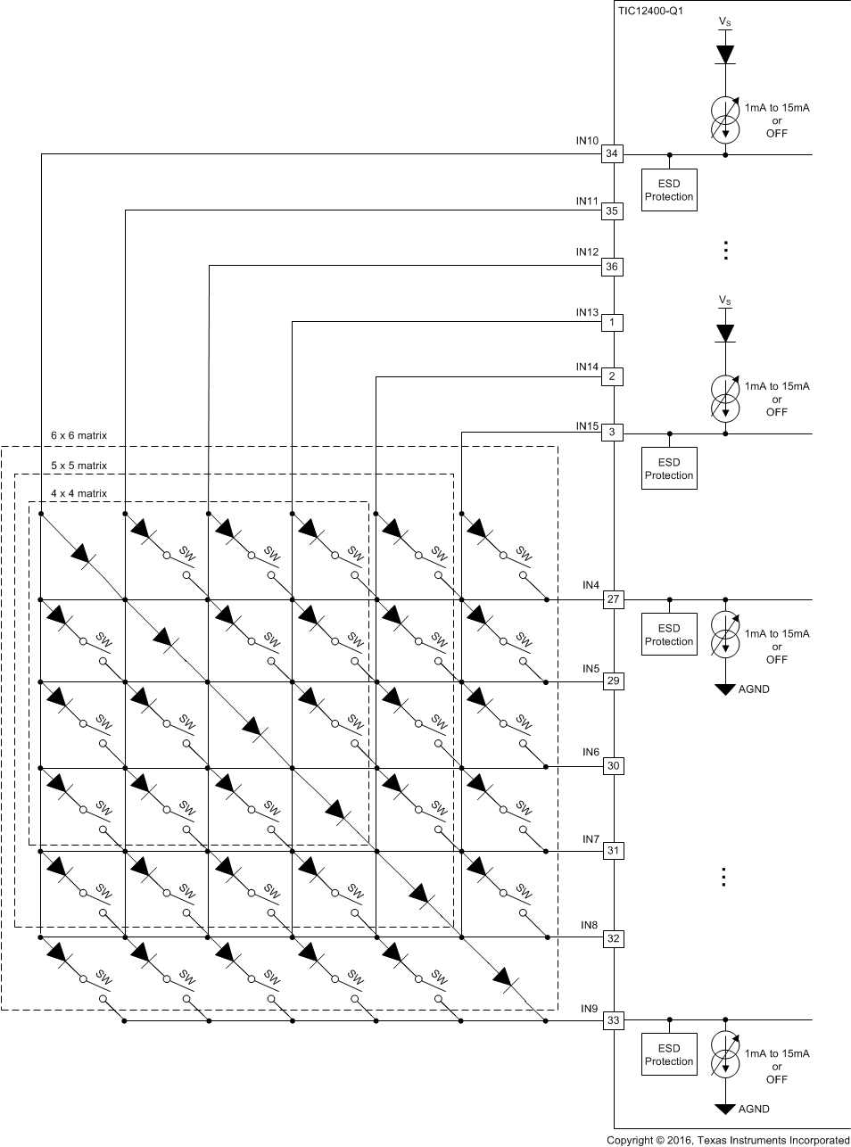
 Figure 8-14 TIC12400-Q1 Matrix Configuration
From IN4 to IN15 a special input switch matrix (see Figure 8-14) can be configured and monitored in addition to the standard switches to GND and VBAT. This feature could be useful to monitor a special switch input configuration called Matrix Inputs as required by some specific OEMs.
Three different matrix configurations are possible, and are defined by MATRIX bits in the MATRIX register. If the MATRIX bits are set to ‘00’ all inputs are treated as standard inputs with identical polling active time according to the POLL_ACT_TIME bits in the CONFIG register. Any settings other than ‘00’ for MATRIX bits causes the polling active time for the matrix inputs to be configured according to POLL_ACT_TIME_M bits in the MATRIX register. Inputs that are not part of the matrix configuration will be configured using the POLL_ACT_TIME bits in the CONFIG register. tPOLL_ACT_TIME_M should be configured properly to allow sufficient time for the current source and sink to charge or discharge the capacitors (if any) connected to the switch inputs.
| Input | 4 x 4 MATRIX | 5 x 5 MATRIX | 6 x 6 MATRIX | |||
|---|---|---|---|---|---|---|
| Current Source Or Sink | Polling Active Time Setting | Current Source Or Sink | Polling Active Time Setting | Current Source Or Sink | Polling Active Time Setting | |
| IN4 | CSI | POLL_ACT_TIME_M | CSI | POLL_ACT_TIME_M | CSI | POLL_ACT_TIME_M |
| IN5 | CSI | CSI | CSI | |||
| IN6 | CSI | CSI | CSI | |||
| IN7 | CSI | CSI | CSI | |||
| IN8 | Configurable to CSO or CSI | POLL_ACT_TIME | CSI | CSI | ||
| IN9 | Configurable to CSO or CSI | Configurable to CSO or CSI | POLL_ACT_TIME | CSI | ||
| IN10 | CSO | POLL_ACT_TIME_M | CSO | POLL_ACT_TIME_M | CSO | |
| IN11 | CSO | CSO | CSO | |||
| IN12 | CSO | CSO | CSO | |||
| IN13 | CSO | CSO | CSO | |||
| IN14 | CSO | POLL_ACT_TIME | CSO | CSO | ||
| IN15 | CSO | CSO | POLL_ACT_TIME | CSO | ||
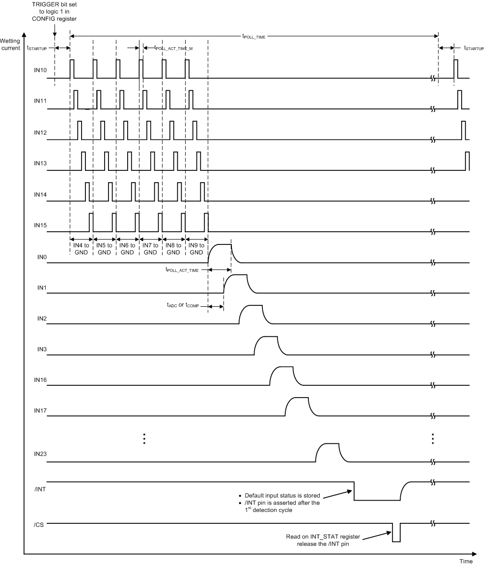
The TIC12400-Q1 implements a different polling scheme when matrix input is configured. After the polling sequence is started (by setting TRIGGER bit in CONFIG register to logic 1), the polling takes place within the matrix input group first before the rest of the standard inputs are polled. After the matrix inputs are polled, the switch status of each input combination (below or above detection threshold) is stored internally in registers IN_STAT_MATRIX0 and IN_STAT_MATRIX1, and it is used as the default state for subsequent matrix polling cycles. The standard inputs follow the same polling behavior as described in section Standard Polling. After the polling cycle is completed on matrix and standard inputs, the INT pin is asserted low to notify the microcontroller that the default switch status is ready to be read. The SSC bit in the INT_STAT register and the SPI status flag SSC are also asserted to logic 1.
The INT_STAT register is cleared and INT pin de-asserted if a SPI READ command is issued to the register. Note: the interrupt is always generated after the 1st complete polling cycle (after the TRIGGER bit in register CONFIG is set to logic 1). In subsequent polling cycles, the interrupt is generated only if switch status change is detected.
Note the following programming requirement when using the matrix polling:
- It is critical to program the CSO/CSI configuration for each matrix input appropriately according to Table 8-6 to avoid incorrect switch status detection.
- It is mandatory to set higher wetting current for the sinks (IN4-IN9) than the sources (IN10-IN15). The actual current flowing through the external switches will be the lesser of the two settings. If the same setting is used for both the sink and the source, the detected result might be incorrect. Because of this, the 15 mA setting shall not be used for the current sources and the 1 mA setting shall not be used for the current sinks. Depending on the type of matrix switches, the TIC12400-Q1 might require some specific wetting current settings to be able to distinguish between switch open or closed states.
- If TW_CUR_DIS_CSO or TW_CUR_DIS_CSI is set to logic 0 in the CONFIG register, wetting current is reduced to 2 mA for 10 mA and 15 mA settings upon TW event. Since it’s mandatory to have higher wetting current for the sinks (IN4-IN9) than the sources (IN10-IN15) during matrix polling, Table 8-7 below summarizes the only possible settings if TW event is expected:
| CSO (IN10-IN15) | CSI (IN4-IN9) | RESULTING WETTING CURRENT |
|---|---|---|
| 1 mA | 2 mA, 5 mA, 10 mA, and 15 mA | 1 mA |
| 2 mA | 5 mA | 2 mA |
If higher wetting current is needed and TW event might be expected, the TW wetting current reduction feature needs to be disabled by setting TW_CUR_DIS_CSO or TW_CUR_DIS_CSI bit in the CONFIG register to 1.
- Only comparator input mode is supported for the matrix polling. Do not program the matrix inputs into ADC input mode. The comparison takes place on the source side (IN10-IN15) since the sink side is pulled to ground. Interrupt generation condition can be set by configuring the INT_EN_COMP1 and INT_EN_COMP2 registers for inputs IN10 to IN15.
Some programmability is removed when matrix polling mode is used, as listed below:
- To keep the polling scheme simple, the ability to disable inputs is removed for the matrix inputs. Only 3 configurations (4×4, 5×5, and 6×6) can be used for the matrix polling. Standard inputs outside the matrix input group can still be disabled, if desired.
- Detection filter (by configuring the DET_FILTER in the CONFIG register) does not apply to the matrix inputs, but still applies to the standard inputs outside the matrix input group.
- When matrix polling is selected, continuous mode is not available to the standard inputs outside the matrix input group.
Figure 8-15 illustrates an example of the polling sequence for the 6×6 matrix input configuration:
 Figure 8-15 Polling Scheme for 6×6 Matrix Inputs
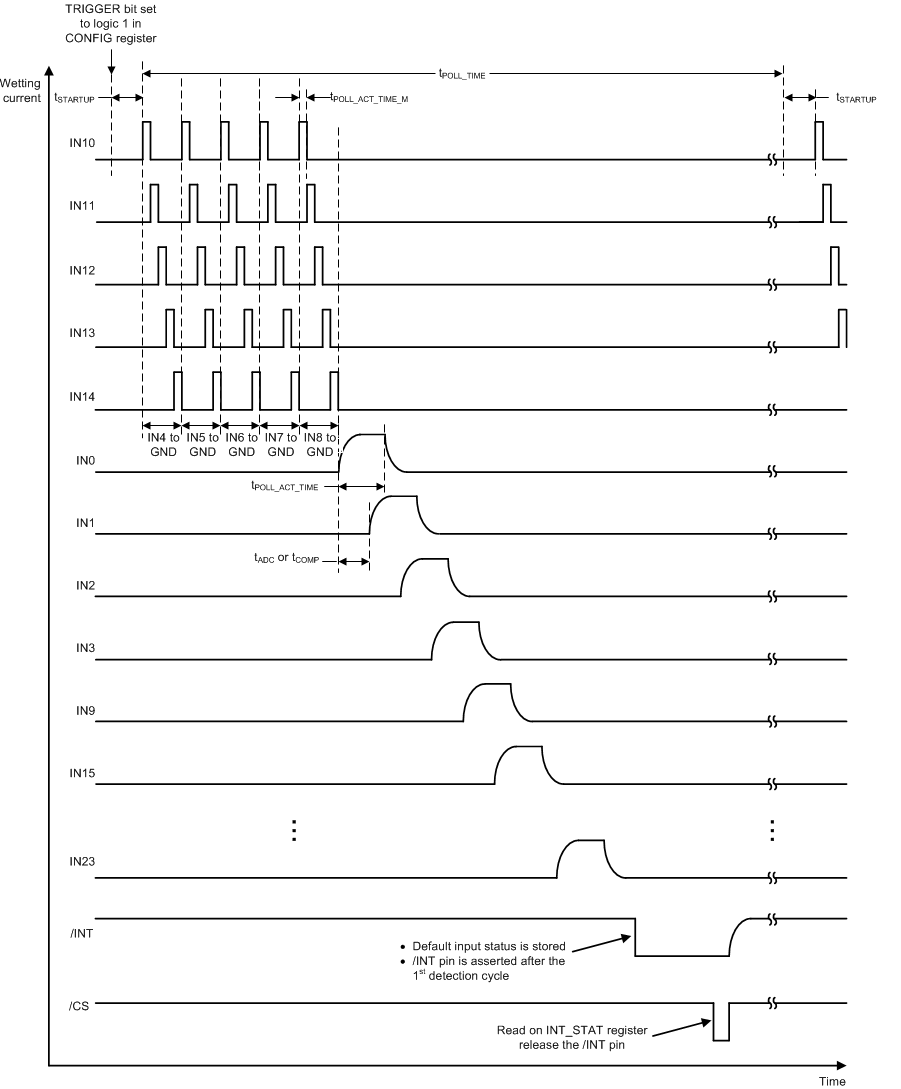
Figure 8-16 illustrates an example of the polling sequence for the 5×5 matrix input configuration. Note: the input IN9 and IN15 are included in the standard polling sequence.
 Figure 8-16 Polling Scheme for 5×5 Matrix Inputs
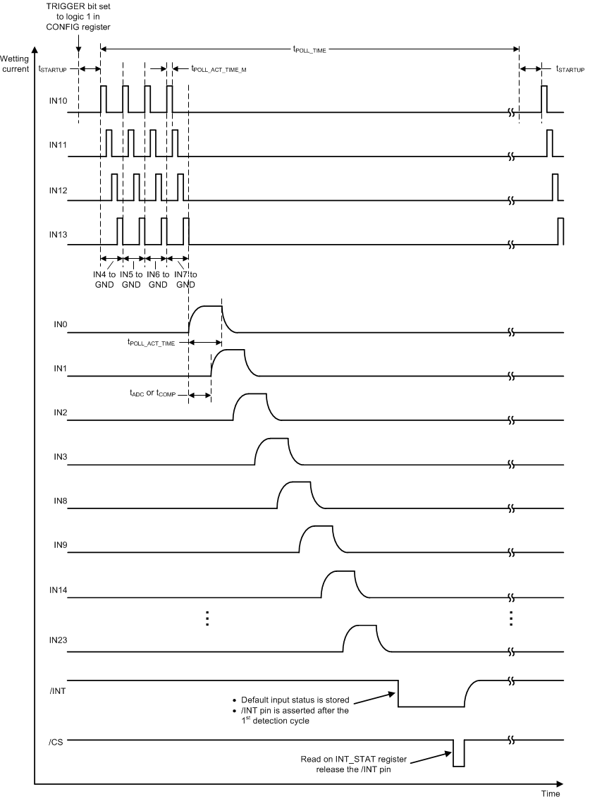
Figure 8-17 illustrates an example of the polling sequence for the 4×4 matrix input configuration. Note: inputs IN8, IN9, IN14, and IN15 are included in the standard polling sequence.
 Figure 8-17 Polling Scheme for 4×4 Matrix Inputs