SLVS062N December 1991 – October 2016 TL1431 , TL1431M
PRODUCTION DATA.
- 1 Features
- 2 Applications
- 3 Description
- 4 Revision History
- 5 Pin Configuration and Functions
- 6 Specifications
- 7 Parameter Measurement Information
- 8 Detailed Description
- 9 Application and Implementation
- 10Power Supply Recommendations
- 11Layout
- 12Device and Documentation Support
- 13Mechanical, Packaging, and Orderable Information
パッケージ・オプション
メカニカル・データ(パッケージ|ピン)
サーマルパッド・メカニカル・データ
発注情報
5 Pin Configuration and Functions
D Package
8-Pin SOIC
Top View
ANODE terminals are connected internally
JG or PW Package
8-Pin CDIP or TSSOP
Top View
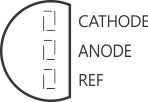
LP Package
3-Pin TO-92
Top View

FK Package
20-Pin LCCC
Top View
Pin Functions
| PIN | I/O | DESCRIPTION | ||||
|---|---|---|---|---|---|---|
| NAME | SOIC | CDIP, TSSOP |
TO-92 | LCCC | ||
| ANODE | 2, 3, 6, 7 | 6 | 2 | 15 | O | Common pin, normally connected to ground |
| CATHODE | 1 | 1 | 1 | 2 | I/O | Shunt current/voltage input |
| REF | 8 | 8 | 3 | 20 | I | Threshold relative to common ground |
| NC | 4, 5 | 2, 3, 4, 5, 7 | — | 1, 3, 4, 5, 6, 7, 8, 9, 10, 11, 12, 13, 14, 16, 17, 18, 19 | — | No internal connection |