SLAS579A April 2009 – June 2015 TLV2553-Q1
PRODUCTION DATA.
- 1 Features
- 2 Applications
- 3 Description
- 4 Revision History
- 5 Pin Configuration and Functions
-
6 Specifications
- 6.1 Absolute Maximum Ratings
- 6.2 ESD Ratings
- 6.3 Recommended Operating Conditions
- 6.4 Thermal Information
- 6.5 Electrical Characteristics
- 6.6 External Reference Specifications
- 6.7 Operating Characteristics
- 6.8 Timing Requirements, VREF+ = 5 V
- 6.9 Timing Requirements, VREF+ = 2.5 V
- 6.10 Typical Characteristics
- 7 Parameter Measurement Information
-
8 Detailed Description
- 8.1 Overview
- 8.2 Functional Block Diagram
- 8.3 Feature Description
- 8.4 Device Functional Modes
- 9 Application and Implementation
- 10Power Supply Recommendations
- 11Layout
- 12Device and Documentation Support
- 13Mechanical, Packaging, and Orderable Information
パッケージ・オプション
メカニカル・データ(パッケージ|ピン)
サーマルパッド・メカニカル・データ
- PW|20
発注情報
6 Specifications
6.1 Absolute Maximum Ratings
over operating free-air temperature range (unless otherwise noted)(1)| MIN | MAX | UNIT | ||
|---|---|---|---|---|
| VCC | Supply voltage(2) | –0.5 | 6.5 | V |
| VI | Input voltage (any input) | –0.3 | VCC + 0.3 | |
| VO | Output voltage | –0.3 | VCC + 0.3 | |
| Vref+ | Positive reference voltage | –0.3 | VCC + 0.3 | |
| Vref– | Negative reference voltage | –0.3 | VCC + 0.3 | |
| II | Peak input current (any input) | –20 | 20 | mA |
| Peak total input current (all inputs) | –30 | 30 | ||
| TJ | Operating virtual junction temperature | –40 | 150 | °C |
| TA | Operating free-air temperature | –40 | 85 | |
| Lead temperature 1.6 mm (1/16 inch) from the case for 10 s | 260 | |||
| Tstg | Storage temperature | –65 | 150 | |
(1) Stresses beyond those listed under Absolute Maximum Ratings may cause permanent damage to the device. These are stress ratings only, and functional operation of the device at these or any other conditions beyond those indicated under Recommended Operating Conditions is not implied. Exposure to absolute-maximum-rated conditions for extended periods may affect device reliability.
(2) All voltage values are with respect to the GND terminal with REF– and GND wired together (unless otherwise noted).
6.2 ESD Ratings
| VALUE | UNIT | |||
|---|---|---|---|---|
| V(ESD) | Electrostatic discharge | Human-body model (HBM), per AEC Q100-002(1) | ±2000 | V |
| Charged-device model (CDM), per AEC Q100-011 | ±500 | |||
(1) AEC Q100-002 indicates that HBM stressing shall be in accordance with the ANSI/ESDA/JEDEC JS-001 specification.
6.3 Recommended Operating Conditions
| MIN | NOM | MAX | UNIT | ||||
|---|---|---|---|---|---|---|---|
| VCC | Supply voltage | 2.7 | 5.5 | V | |||
| I/O CLOCK frequency | VCC = 4.5 V to 5.5 V | 16-bit I/O | 0.01 | 15 | MHz | ||
| 12-bit I/O | 0.01 | 15 | |||||
| 18-bit I/O | 0.01 | 15 | |||||
| VCC = 2.7 to 3.6 V | 0.01 | 10 | |||||
| Tolerable clock jitter, I/O CLOCK | VCC = 4.5 V to 5.5 V | 0.38 | ns | ||||
| Aperature jitter | VCC = 4.5 V to 5.5 V | 100 | ps | ||||
| Analog input voltage(1) | VCC = 4.5 V to 5.5 V | 0 | REF+ – REF– | V | |||
| VCC = 3 V to 3.6 V | 0 | ||||||
| VCC = 2.7 V to 3 V | 0 | ||||||
| VIH | High-level control input voltage | VCC = 4.5 V to 5.5 V | 2 | V | |||
| VCC = 2.7 V to 3.6 V | 2.1 | ||||||
| VIL | Low-level control input voltage | VCC = 4.5 V to 5.5 V | 0.8 | V | |||
| VCC = 2.7 V to 3.6 V | 0.6 | ||||||
| TA | Operating free-air temperature | –40 | 85 | °C | |||
(1) Analog input voltages greater than the voltage applied to REF+ convert as all ones (111111111111), while input voltages less than the voltage applied to REF– convert as all zeros (000000000000).
6.4 Thermal Information
| THERMAL METRIC(1) | TLV2553-Q1 | UNIT | ||
|---|---|---|---|---|
| DW (SOIC) | PW (TSSOP) | |||
| 20 PINS | 20 PINS | |||
| RθJA | Junction-to-ambient thermal resistance | 66.0 | 88.1 | °C/W |
| RθJC(top) | Junction-to-case (top) thermal resistance | 31.4 | 21.6 | °C/W |
| RθJB | Junction-to-board thermal resistance | 33.7 | 40.4 | °C/W |
| ψJT | Junction-to-top characterization parameter | 7.4 | 0.8 | °C/W |
| ψJB | Junction-to-board characterization parameter | 33.3 | 39.7 | °C/W |
| RθJC(bot) | Junction-to-case (bottom) thermal resistance | N/A | N/A | °C/W |
(1) For more information about traditional and new thermal metrics, see the Semiconductor and IC Package Thermal Metrics application report, SPRA953.
6.5 Electrical Characteristics
over recommended operating free-air temperature range, when VCC = 5 V: VREF+ = 5 V, I/O CLOCK frequency = 15 MHz,when VCC = 2.7 V: VREF+ = 2.5 V, I/O CLOCK frequency = 10 MHz (unless otherwise noted)
| PARAMETER | TEST CONDITIONS | MIN | TYP(1) | MAX | UNIT | ||||
|---|---|---|---|---|---|---|---|---|---|
| VOH | High-level output voltage | VCC = 4.5 V, IOH = –1.6 mA VCC = 2.7 V, IOH = –0.2 mA |
30 pF | 2.4 | V | ||||
| VCC = 4.5 V, IOH = –20 μA VCC = 2.7 V, IOH = –20 μA |
VCC – 0.1 | ||||||||
| VOL | Low-level output voltage | VCC = 4.5 V, IOL = –1.6 mA VCC = 2.7 V, IOL = –0.8 mA |
30 pF | 0.4 | V | ||||
| VCC = 4.5 V, IOL = –20 μA VCC = 2.7 V, IOL = –20 μA |
0.1 | ||||||||
| IOZ | High-impedance off-state output current | VO = VCC, CS = VCC | 1 | 2.5 | μA | ||||
| VO = 0 V, CS = VCC | –1 | –2.5 | |||||||
| ICC | Operating supply current | CS = 0 V, External reference | VCC = 5 V | 1.2 | mA | ||||
| VCC = 2.7 V | 0.9 | ||||||||
| ICC(PD) | Power-down current | For all digital inputs, 0 ≤ VI ≤ 0.5 V or VI ≥ VCC – 0.5 V, I/O CLOCK = 0 V | Software power down | 0.1 | 1 | μA | |||
| Auto power down | 0.1 | 10 | |||||||
| IIH | High-level input current | VI = VCC | 0.005 | 2.5 | μA | ||||
| IIL | Low-level input current | VI = 0 V | –0.005 | –2.5 | μA | ||||
| Ilkg | Selected channel leakage current | Selected channel at VCC , Unselected channel at 0 V |
1 | μA | |||||
| Selected channel at 0 V, Unselected channel at VCC |
–1 | ||||||||
| fOSC | Internal oscillator frequency | VCC = 4.5 V to 5.5 V | 3.27 | MHz | |||||
| VCC = 2.7 V to 3.6 V | 2.56 | ||||||||
| tconvert | Conversion time (13.5 × (1/fOSC) + 25 ns) |
VCC = 4.5 V to 5.5 V | 4.15 | μs | |||||
| VCC = 2.7 V to 3.6 V | 5.54 | ||||||||
| Internal oscillator frequency voltage | 3.6 | 4.1 | V | ||||||
| Zi | Input impedance(2) | Analog inputs | VCC = 4.5 V | 500 | Ω | ||||
| VCC = 2.7 V | 600 | ||||||||
| Ci | Input capacitance | Analog inputs | 45 | 55 | pF | ||||
| Control inputs | 5 | 15 | |||||||
(1) All typical values are at VCC = 5 V, TA = 25°C.
(2) The switch resistance is very nonlinear and varies with input voltage and supply voltage. This is the worst case.
6.6 External Reference Specifications(2)
| PARAMETER | TEST CONDITIONS | MIN | TYP(1) | MAX | UNIT | ||
|---|---|---|---|---|---|---|---|
| VREF– | Reference input voltage, REF– | VCC = 4.5 V to 5.5 V | –0.1 | 0 | 0.1 | V | |
| VCC = 2.7 V to 3.6 V | –0.1 | 0 | 0.1 | ||||
| VREF+ | Reference input voltage, REF+ | VCC = 4.5 V to 5.5 V | 2 | VCC | V | ||
| VCC = 2.7 V to 3.6 V | 2 | VCC | |||||
| External reference input voltage difference (REF+ – REF–) | VCC = 4.5 V to 5.5 V | 1.9 | VCC | V | |||
| VCC = 2.7 V to 3.6 V | 1.9 | VCC | |||||
| IREF | External reference supply current | CS = 0 V | VCC = 4.5 V to 5.5 V | 0.94 | mA | ||
| VCC = 2.7 V to 3.6 V | 0.62 | ||||||
| ZREF | Reference input impedance | VCC = 5 V | Static | 1 | MΩ | ||
| During sampling/conversion | 6 | 9 | kΩ | ||||
| VCC = 2.7 V | Static | 1 | MΩ | ||||
| During sampling/conversion | 6 | 9 | kΩ | ||||
(1) All typical values are at VCC = 5 V, TA = 25°C.
(2) Add a 0.1-μF capacitor between REF+ and REF– pins when external reference is used.
6.7 Operating Characteristics
over recommended operating free-air temperature range, when VCC = 5 V: VREF+ = 5 V, I/O CLOCK frequency = 15 MHz,when VCC = 2.7 V: VREF+ = 2.5 V, I/O CLOCK frequency = 10 MHz (unless otherwise noted)
| PARAMETER | TEST CONDITIONS | MIN | TYP(1) | MAX | UNIT | |
|---|---|---|---|---|---|---|
| INL | Integral linearity error(3) | –1 | 1 | LSB | ||
| DNL | Differential linearity error | –1 | 1 | LSB | ||
| EO | Offset error(4) | See (2) | –2 | 2 | mV | |
| EG | Gain error(4) | See (2) | –3 | 3 | mV | |
| ET | Total unadjusted error(5) | ±1.5 | LSB | |||
| Self-test output code(6) (see Table 2 and Table 3) | Address data input = 1011 | 2048 | ||||
| Address data input = 1100 | 0 | |||||
| Address data input = 1101 | 4095 | |||||
(1) All typical values are at VCC = 5 V, TA = 25°C.
(2) Analog input voltages greater than the voltage applied to REF+ convert as all ones (111111111111), while input voltages less than the voltage applied to REF– convert as all zeros (000000000000).
(3) Linearity error is the maximum deviation from the best straight line through the A/D transfer characteristics.
(4) Gain error is the difference between the actual midstep value and the nominal midstep value in the transfer diagram at the specified gain point after the offset error has been adjusted to zero. Offset error is the difference between the actual midstep value and the nominal midstep value at the offset point.
(5) Total unadjusted error comprises linearity, zero-scale errors, and full-scale errors.
(6) Both the input address and the output codes are expressed in positive logic.
6.8 Timing Requirements, VREF+ = 5 V
over recommended operating free-air temperature range,VREF+ = 5 V, I/O CLOCK frequency = 15 MHz, VCC = 5 V, Load = 25 pF (unless otherwise noted)
| MIN | MAX | UNIT | |||
|---|---|---|---|---|---|
| tw1 | Pulse duration I/O CLOCK high or low | 26.7 | 100000 | ns | |
| tsu1 | Setup time DATA IN valid before I/O CLOCK rising edge (see Figure 26) | 12 | ns | ||
| th1 | Hold time DATA IN valid after I/O CLOCK rising edge (see Figure 26) | 0 | ns | ||
| tsu2 | Setup time CS low before first rising I/O CLOCK edge(2) (see Figure 27) | 25 | ns | ||
| th2 | Hold time CS pulse duration high time (see Figure 27) | 100 | ns | ||
| th3 | Hold time CS low after last I/O CLOCK falling edge (see Figure 27) | 0 | ns | ||
| th4 | Hold time DATA OUT valid after I/O CLOCK falling edge (see Figure 28) | 2 | ns | ||
| th5 | Hold time CS high after EOC rising edge when CS is toggled (see Figure 31) | 0 | ns | ||
| td1 | Delay time CS falling edge to DATA OUT valid (MSB or LSB) (see Figure 25) | Load = 25 pF | 28 | ns | |
| Load = 10 pF | 20 | ||||
| td2 | Delay time CS rising edge to DATA OUT high impedance (see Figure 25) | 10 | ns | ||
| td3 | Delay time I/O CLOCK falling edge to next DATA OUT bit valid (see Figure 28) | 2 | 20 | ns | |
| td4 | Delay time last I/O CLOCK falling edge to EOC falling edge | 55 | ns | ||
| td5 | Delay time last I/O CLOCK falling edge to CS falling edge to abort conversion | 1.5 | μs | ||
| tt1 | Transition time I/O CLOCK(2) (see Figure 28) | 1 | μs | ||
| tt2 | Transition time DATA OUT (see Figure 28) | 5 | ns | ||
| tt3 | Transition time EOC, CL = 7 pF (see Figure 30) | 2.4 | ns | ||
| tt4 | Transition time DATA IN, CS | 10 | μs | ||
| tcycle | Total cycle time (sample, conversion and delays)(2) | (1) | μs | ||
| tsample | Channel acquisition time (sample) at 1 kΩ(2)
(see Figure 33 through Figure 38) |
Source impedance = 25 Ω | 600 | ns | |
| Source impedance = 100 Ω | 650 | ||||
| Source impedance = 500 Ω | 700 | ||||
| Source impedance = 1 kΩ | 1000 | ||||
(1) tconvert(max) + I/O CLOCK period (8/12/16 CLKs)(2)
(2) I/O CLOCK period = 8 × [1/(I/O CLOCK frequency)] or 12 × [1/(I/O CLOCK frequency)] or 16 × [1/(I/O CLOCK frequency)], depending on I/O format selected
6.9 Timing Requirements, VREF+ = 2.5 V
over recommended operating free-air temperature range,VREF+ = 2.5 V, I/O CLOCK frequency = 10 MHz, VCC = 2.7 V, Load = 25 pF (unless otherwise noted)
| MIN | MAX | UNIT | |||
|---|---|---|---|---|---|
| tw1 | Pulse duration I/O CLOCK high or low | 40 | 100000 | ns | |
| tsu1 | Setup time DATA IN valid before I/O CLOCK rising edge (see Figure 26) | 22 | ns | ||
| th1 | Hold time DATA IN valid after I/O CLOCK rising edge (see Figure 26) | 0 | ns | ||
| tsu2 | Setup time CS low before first rising I/O CLOCK edge(2) (see Figure 27) | 33 | ns | ||
| th2 | Hold time CS pulse duration high time (see Figure 27) | 100 | ns | ||
| th3 | Hold time CS low after last I/O CLOCK falling edge (see Figure 27) | 0 | ns | ||
| th4 | Hold time DATA OUT valid after I/O CLOCK falling edge (see Figure 28) | 2 | ns | ||
| th5 | Hold time CS high after EOC rising edge when CS is toggled (see Figure 31) | 0 | ns | ||
| td1 | Delay time CS falling edge to DATA OUT valid (MSB or LSB) (see Figure 25) | Load = 25 pF | 30 | ns | |
| Load = 10 pF | 22 | ||||
| td2 | Delay time CS rising edge to DATA OUT high impedance (see Figure 25) | 10 | ns | ||
| td3 | Delay time I/O CLOCK falling edge to next DATA OUT bit valid (see Figure 28) | 2 | 33 | ns | |
| td4 | Delay time last I/O CLOCK falling edge to EOC falling edge | 75 | ns | ||
| td5 | Delay time last I/O CLOCK falling edge to CS falling edge to abort conversion | 1.5 | μs | ||
| tt1 | Transition time I/O CLOCK(2) (see Figure 28) | 1 | μs | ||
| tt2 | Transition time DATA OUT (see Figure 28) | 5 | ns | ||
| tt3 | Transition time EOC, CL = 7 pF (see Figure 30) | 4 | ns | ||
| tt4 | Transition time DATA IN, CS | 10 | μs | ||
| tcycle | Total cycle time (sample, conversion and delays)(2) | (1) | μs | ||
| tsample | Channel acquisition time (sample), at 1 kΩ(2)
(see Figure 33 through Figure 38) |
Source impedance = 25 Ω | 800 | ns | |
| Source impedance = 100 Ω | 850 | ||||
| Source impedance = 500 Ω | 1000 | ||||
| Source impedance = 1 kΩ | 1600 | ||||
(1) tconvert(max) + I/O CLOCK period (8/12/16 CLKs)(2)
(2) I/O CLOCK period = 8 × [1/(I/O CLOCK frequency)] or 12 × [1/(I/O CLOCK frequency)] or 16 × [1/(I/O CLOCK frequency)], depending on I/O format selected
6.10 Typical Characteristics
VREF– = 0 V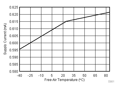
| VCC = 3.3 V | VREF+ = 2.5 V | I/O clock = 10 MHz |
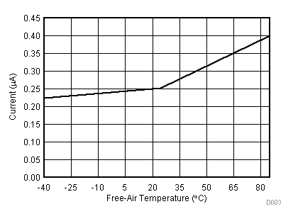
| VCC = 3.3 V | VREF+ = 2.5 V | I/O clock = 10 MHz |
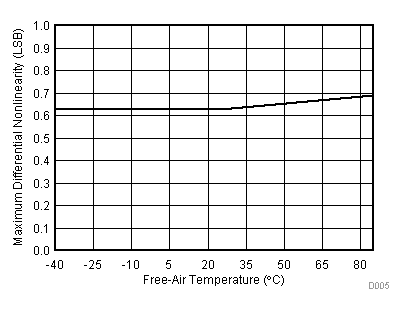
| VCC = 2.7 V | VREF+ = 2.5 V | I/O clock = 10 MHz |
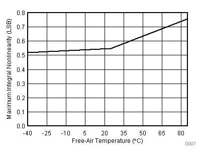
| VCC = 2.7 V | VREF+ = 2.5 V | I/O clock = 10 MHz |
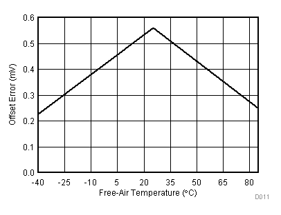
| VCC = 3.3 V | VREF+ = 2.5 V | I/O clock = 10 MHz |
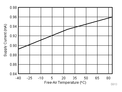
| VCC = 5.5 V | VREF+ = 4.096 V | I/O clock = 15 MHz |
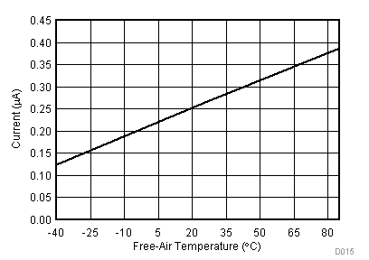
| VCC = 5.5 V | VREF+ = 4.096 V | I/O clock = 15 MHz |
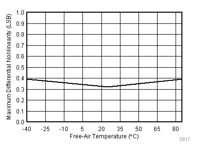
| VCC = 5.5 V | VREF+ = 4.096 V | I/O clock = 15 MHz |
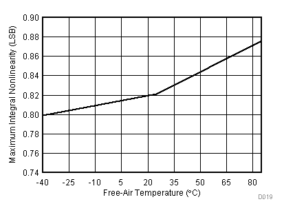
| VCC = 5.5 V | VREF+ = 4.096 V | I/O clock = 15 MHz |
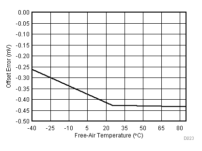
| VCC = 5.5 V | VREF+ = 4.096 V | I/O clock = 15 MHz |
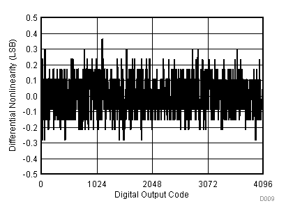
| VCC = 2.7 V | VREF+ = 2.5 V | I/O clock = 10 MHz |
| TA = 25°C |
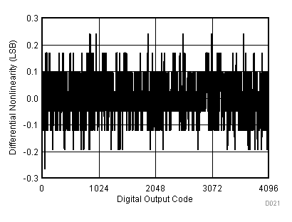
| VCC = 5.5 V | VREF+ = 4.096 V | I/O clock = 15 MHz |
| TA = 25°C |
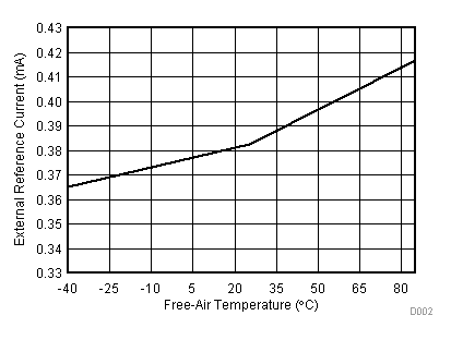
| VCC = 3.3 V | VREF+ = 2.5 V | I/O clock = 10 MHz |
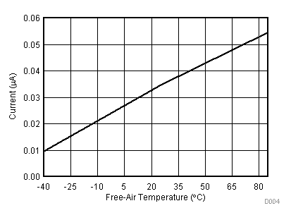
| VCC = 3.3 V | VREF+ = 2.5 V | I/O clock = 10 MHz |
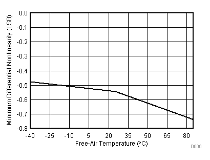
| VCC = 2.7 V | VREF+ = 2.5 V | I/O clock = 10 MHz |
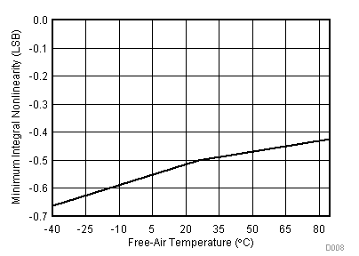
| VCC = 2.7 V | VREF+ = 2.5 V | I/O clock = 10 MHz |
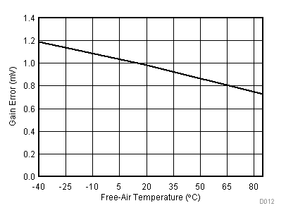
| VCC = 3.3 V | VREF+ = 2.5 V | I/O clock = 10 MHz |
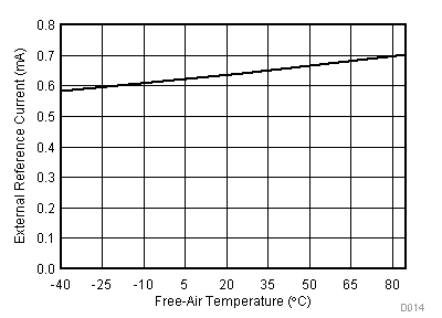
| VCC = 5.5 V | VREF+ = 4.096 V | I/O clock = 15 MHz |
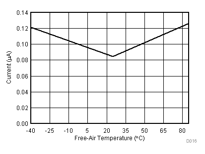
| VCC = 5.5 V | VREF+ = 4.096 V | I/O clock = 15 MHz |
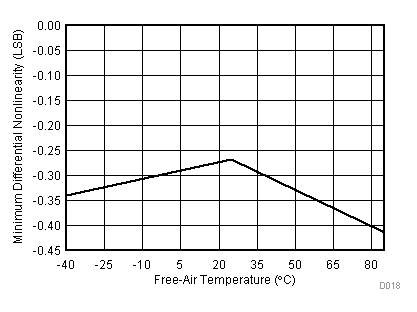
| VCC = 5.5 V | VREF+ = 4.096 V | I/O clock = 15 MHz |
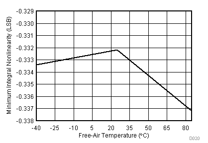
| VCC = 5.5 V | VREF+ = 4.096 V | I/O clock = 15 MHz |
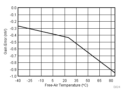
| VCC = 5.5 V | VREF+ = 4.096 V | I/O clock = 15 MHz |
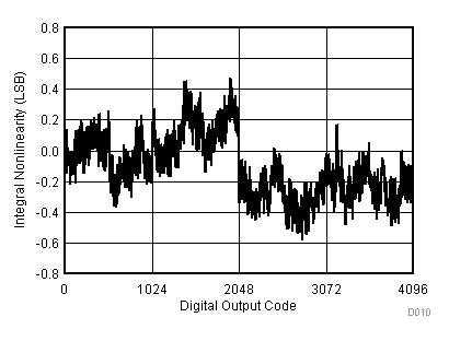
| VCC = 2.7 V | VREF+ = 2.5 V | I/O clock = 10 MHz |
| TA = 25°C |
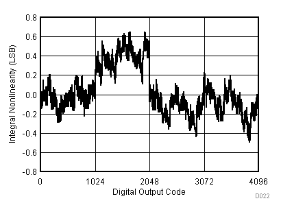
| VCC = 5.5 V | VREF+ = 4.096 V | I/O clock = 15 MHz |
| TA = 25°C |