JAJSJB1D June   2021  – July 2022 TLV3601-Q1 , TLV3602-Q1 , TLV3603-Q1

PRODMIX  

  1. 特長
  2. アプリケーション
  3. 概要
  4. Revision History
  5. Pin Configuration and Functions
  6. Specifications
    1. 6.1 Absolute Maximum Ratings
    2. 6.2 ESD Ratings
    3. 6.3 Recommended Operating Conditions
    4. 6.4 Thermal Information
    5. 6.5 Electrical Characteristics
    6. 6.6 Timing Diagrams
    7. 6.7 Typical Characteristics
  7. Detailed Description
    1. 7.1 Overview
    2. 7.2 Functional Block Diagram
    3. 7.3 Feature Description
    4. 7.4 Device Functional Modes
      1. 7.4.1 Inputs
      2. 7.4.2 Push-Pull (Single-Ended) Output
      3. 7.4.3 Known Startup Condition
  8. Application and Implementation
    1. 8.1 Application Information
      1. 8.1.1 Adjustable Hysteresis
      2. 8.1.2 Capacitive Loads
      3. 8.1.3 Latch Functionality
    2. 8.2 Typical Application
      1. 8.2.1 Implementing Hysteresis
        1. 8.2.1.1 Design Requirements
        2. 8.2.1.2 Detailed Design Procedure
        3. 8.2.1.3 Application Curve
      2. 8.2.2 Optical Receiver
      3. 8.2.3 Over-Current Latch Condition
      4. 8.2.4 External Trigger Function for Oscilloscopes
  9. Power Supply Recommendations
  10. 10Layout
    1. 10.1 Layout Guidelines
    2. 10.2 Layout Example
  11. 11Device and Documentation Support
    1. 11.1 Device Support
      1. 11.1.1 Development Support
    2. 11.2 Receiving Notification of Documentation Updates
    3. 11.3 サポート・リソース
    4. 11.4 Trademarks
    5. 11.5 Electrostatic Discharge Caution
    6. 11.6 Glossary
  12. 12Mechanical, Packaging, and Orderable Information

パッケージ・オプション

メカニカル・データ(パッケージ|ピン)
サーマルパッド・メカニカル・データ
発注情報

Typical Characteristics

At TA = 25°C, VCC - VEE = 2.5 V to 5 V, VCM = 300 mV, RHYST = 150 kΩ (TLV3603-Q1 only), and input overdrive = 50 mV, unless otherwise noted.

Figure 6-3 TLV3601 Offset vs. Temperature
Figure 6-5 TLV3601 Offset vs. Common-Mode, 2.5 V
Figure 6-7 TLV3601 Offset vs. Common-Mode, 3.3 V
Figure 6-9 TLV3601 Offset vs. Common-Mode, 5 V
Figure 6-11 TLV3603 Offset vs. Temperature
Figure 6-13 TLV3603 Offset vs. Common-Mode, 2.5 V
Figure 6-15 TLV3603 Offset vs. Common-Mode, 3.3 V
Figure 6-17 TLV3603 Offset vs. Common-Mode, 5 V
Figure 6-19 TLV3603 Hysteresis vs. Resistance, 2.5 V
Figure 6-21 TLV3603 Hysteresis vs. Resistance, 5 V
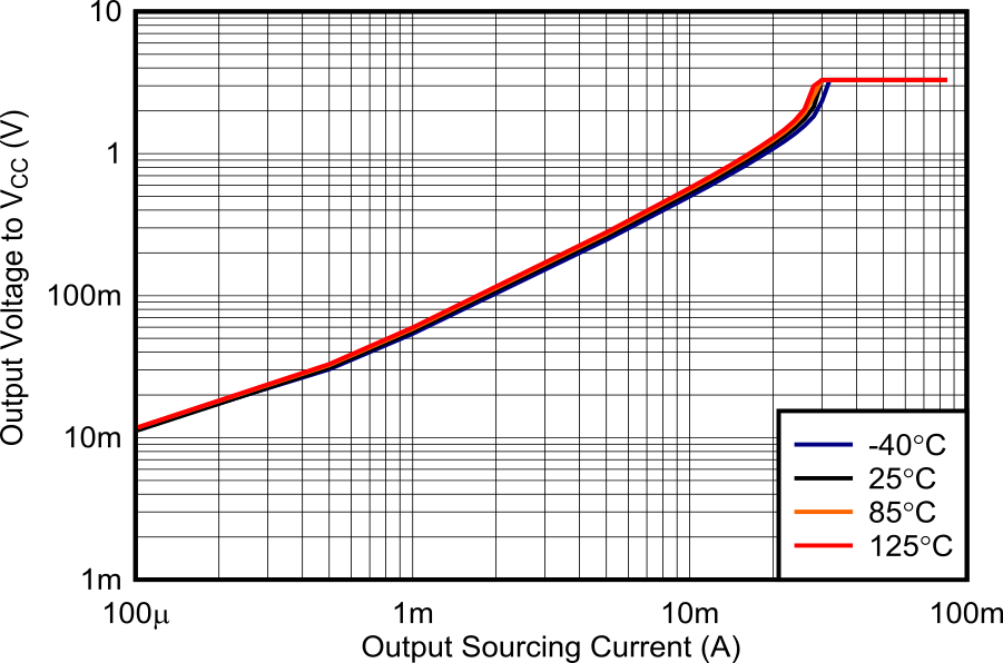
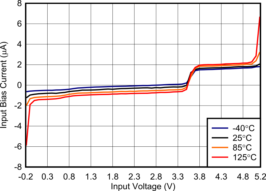
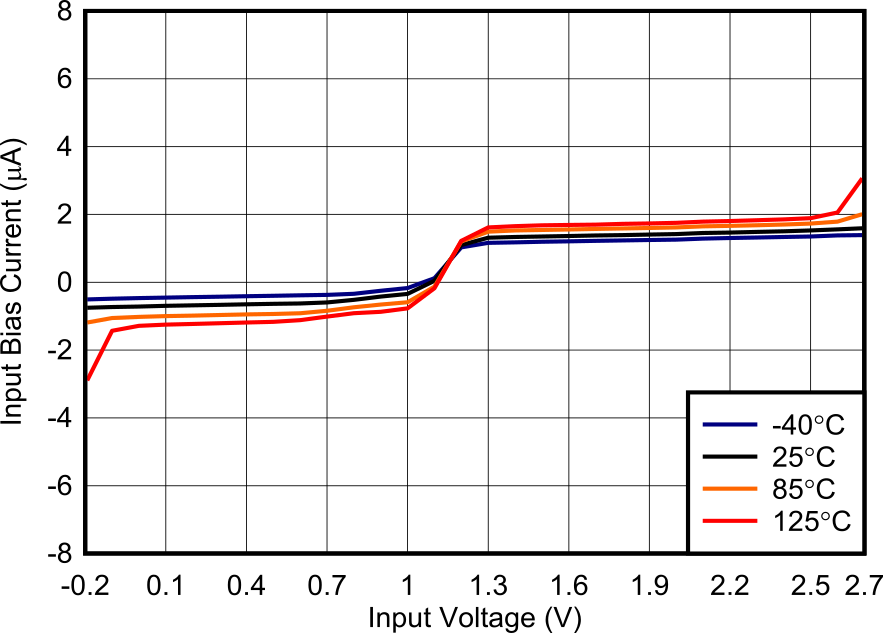
Figure 6-23 Bias Current vs. Input Voltage, 3.3 V
Figure 6-25 Output Voltage vs. Output Sourcing Current, 2.5 V
GUID-20210811-SS0I-Q9SK-SX38-JSCZGTSZBRDX-low.png
Figure 6-27 Output Voltage vs. Output Sourcing Current, 3.3 V
GUID-20210811-SS0I-VJ7P-GBWR-04XKNCBDR0FQ-low.png
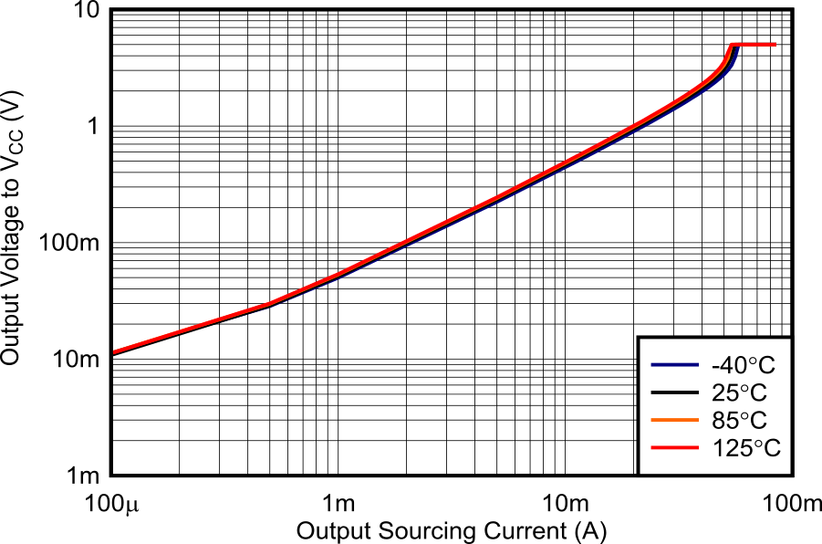
Figure 6-29 Output Voltage vs. Output Sourcing Current, 5 V
Figure 6-31 TLV3601 Supply Current vs. Voltage (Output Low)
GUID-20210811-SS0I-JSMV-6TTF-H07DVBX2K43Q-low.png
Figure 6-33 TLV3601 Supply Current vs. Temp (Output Low)
Figure 6-35 TLV3603 Supply Current vs. Voltage (Output Low)
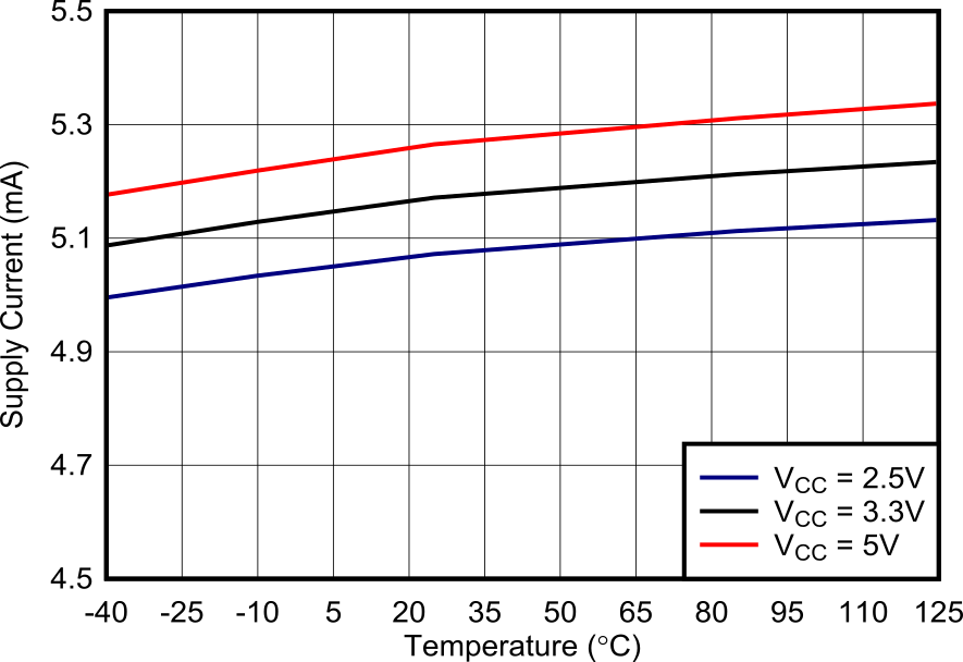
Figure 6-37 TLV3603 Supply Current vs. Temp (Output Low)
Figure 6-39 Propagation Delay, Low to High, 2.5 V
GUID-20210811-SS0I-QFQG-SQQW-R5MHBS3PBWFQ-low.png
Figure 6-41 Propagation Delay, Low to High, 3.3 V
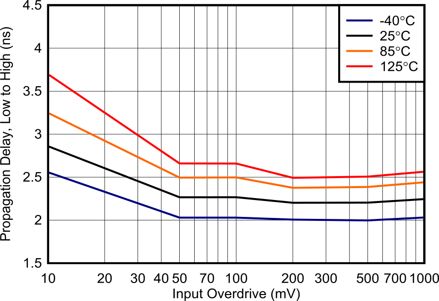
GUID-20210811-SS0I-MG3H-Z9JZ-7LCKD9TSRFCN-low.pngFigure 6-43 Propagation Delay, Low to High, 5 V
Figure 6-45 Propagation Delay vs. Load Capacitance, 3.3 V
GUID-20210811-SS0I-BXPK-XPMP-CRK1GNL4FTJC-low.pngFigure 6-47 Minimum Pulse Width vs. Temperature.
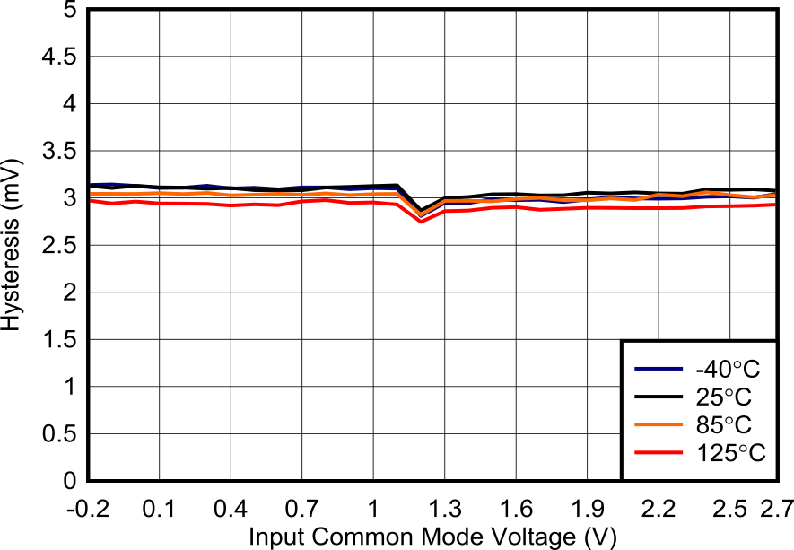
Figure 6-4 TLV3601 Hysteresis vs. Temperature
GUID-20210811-SS0I-JL3X-F022-2MXJQD6ZVTK5-low.png
Figure 6-6 TLV3601 Hysteresis vs. Common-Mode, 2.5 V
Figure 6-8 TLV3601 Hysteresis vs. Common-Mode, 3.3 V
Figure 6-10 TLV3601 Hysteresis vs. Common-Mode, 5 V
Figure 6-12 TLV3603 Hysteresis vs. Temperature
Figure 6-14 TLV3603 Hysteresis vs. Common-Mode, 2.5 V
Figure 6-16 TLV3603 Hysteresis vs. Common-Mode, 3.3 V
Figure 6-18 TLV3603 Hysteresis vs. Common-Mode, 5 V
Figure 6-20 TLV3603 Hysteresis vs. Resistance, 3.3 V
GUID-20210811-SS0I-KPWX-PBXZ-QRTV2SBZJVB0-low.png
Figure 6-22 Bias Current vs. Input Voltage, 2.5 V
GUID-20210811-SS0I-VGGV-T0C3-XHBXFTFRS5KK-low.png
Figure 6-24 Bias Current vs. Input Voltage, 5 V
GUID-20210811-SS0I-V9KQ-HCDX-DQWRTGJN7TCD-low.png
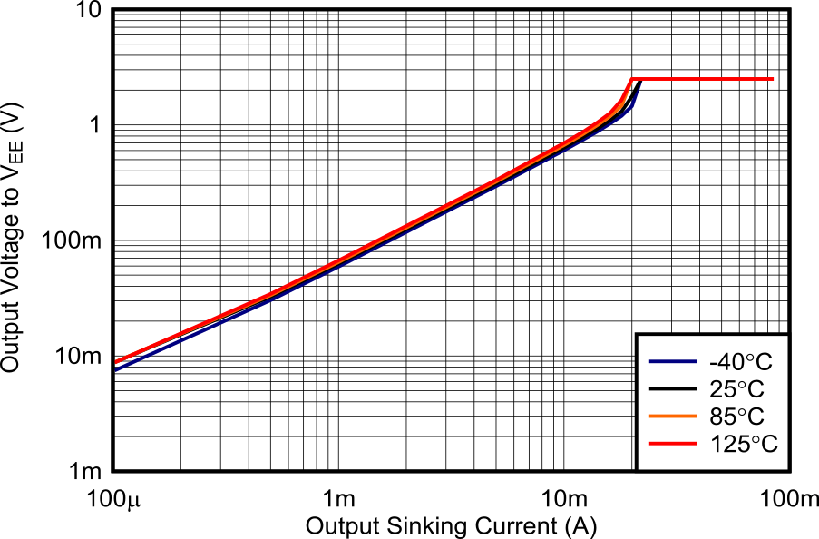
Figure 6-26 Output Voltage vs. Output Sinking Current, 2.5 V
GUID-20210811-SS0I-GKTF-L1TK-6F20H6SWMJPQ-low.png
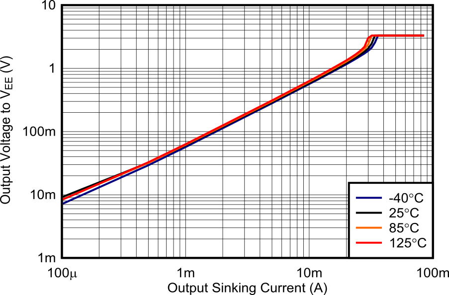
Figure 6-28 Output Voltage vs. Output Sinking Current, 3.3 V
GUID-20210811-SS0I-GGMH-6SMB-Q08W1MS3FFFF-low.png
Figure 6-30 Output Voltage vs. Output Sinking Current, 5 V
Figure 6-32 TLV3601 Supply Current vs. Voltage (Output High)
GUID-20210809-SS0I-PS0X-VNRW-BL9FQTK54N4K-low.png
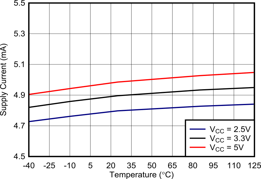
Figure 6-34 TLV3601 Supply Current vs. Temp (Output High)
Figure 6-36 TLV3603 Supply Current vs. Voltage (Output High)
Figure 6-38 TLV3603 Supply Current vs. Temp (Output High)
Figure 6-40 Propagation Delay, High to Low, 2.5 V
Figure 6-42 Propagation Delay, High to Low, 3.3 V
GUID-20210811-SS0I-F0RT-6LM6-7G3M88JG5DVP-low.pngFigure 6-44 Propagation Delay, High to Low, 5 V
Figure 6-46 Propagation Delay vs. Load Capacitance, 5 V