SLVS905A December 2008 – October 2017 TLV431A-Q1 , TLV431B-Q1
PRODUCTION DATA.
- 1 Features
- 2 Applications
- 3 Description
- 4 Revision History
- 5 Pin Configuration and Functions
- 6 Specifications
- 7 Parameter Measurement Information
- 8 Detailed Description
- 9 Applications and Implementation
- 10Power Supply Recommendations
- 11Layout
- 12Device and Documentation Support
- 13Mechanical, Packaging, and Orderable Information
パッケージ・オプション
メカニカル・データ(パッケージ|ピン)
サーマルパッド・メカニカル・データ
発注情報
8 Detailed Description
8.1 Overview
TLV431 is a low power counterpart to TL431, having lower reference voltage (1.24 V vs 2.5 V) for lower voltage adjustability and lower minimum cathode current (Ik(min)=100 µA vs 1 mA). Like TL431, the TLV431 is used in conjunction with it's key components to behave as a single voltage reference, error amplifier, voltage clamp or comparator with integrated reference.
TLV431 can be operated and adjusted to cathode voltages from 1.24V to 6V, making this part optimum for a wide range of end equipments in industrial, auto, telecom & computing. In order for this device to behave as a shunt regulator or error amplifier, > 100 µA (Imin(max)) must be supplied in to the cathode pin. Under this condition, feedback can be applied from the Cathode and Ref pins to create a replica of the internal reference voltage.
Various reference voltage options can be purchased with initial tolerances (at 25°C) of 0.5%, and 1%. These reference options are denoted by B (0.5%) and A (1.0%) after the TLV431x-Q1.
The TLV431x-Q1 devices are characterized for operation from –40°C to 125°C.
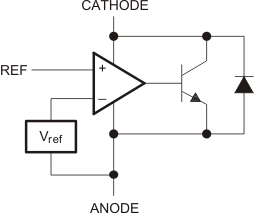
8.2 Functional Block Diagram

8.3 Feature Description
TLV431 consists of an internal reference and amplifier that outputs a sink current base on the difference between the reference pin and the virtual internal pin. The sink current is produced by an internal darlington pair.
When operated with enough voltage headroom (≥ 1.24 V) and cathode current (Ika), TLV431 forces the reference pin to 1.24 V. However, the reference pin can not be left floating, as it needs Iref ≥ 0.5 µA (please see the Functional Block Diagram). This is because the reference pin is driven into an npn, which needs base current in order operate properly.
When feedback is applied from the Cathode and Reference pins, TLV431 behaves as a Zener diode, regulating to a constant voltage dependent on current being supplied into the cathode. This is due to the internal amplifier and reference entering the proper operating regions. The same amount of current needed in the above feedback situation must be applied to this device in open loop, servo or error amplifying implementations in order for it to be in the proper linear region giving TLV431 enough gain.
Unlike many linear regulators, TLV431 is internally compensated to be stable without an output capacitor between the cathode and anode. However, if it is desired to use an output capacitor Figure 18 can be used as a guide to assist in choosing the correct capacitor to maintain stability.
8.4 Device Functional Modes
8.4.1 Open Loop (Comparator)
When the cathode/output voltage or current of TLV431 is not being fed back to the reference/input pin in any form, this device is operating in open loop. With proper cathode current (Ika) applied to this device, TLV431 will have the characteristics shown in Figure 6. With such high gain in this configuration, TLV431 is typically used as a comparator. With the reference integrated makes TLV431 the preferred choice when users are trying to monitor a certain level of a single signal.
8.4.2 Closed Loop
When the cathode/output voltage or current of TLV431 is being fed back to the reference/input pin in any form, this device is operating in closed loop. The majority of applications involving TLV431 use it in this manner to regulate a fixed voltage or current. The feedback enables this device to behave as an error amplifier, computing a portion of the output voltage and adjusting it to maintain the desired regulation. This is done by relating the output voltage back to the reference pin in a manner to make it equal to the internal reference voltage, which can be accomplished via resistive or direct feedback.