JAJSIO2G March 2020 – March 2022 TLV9041 , TLV9042 , TLV9044
PRODUCTION DATA
- 1 特長
- 2 アプリケーション
- 3 概要
- 4 Revision History
- 5 Device Comparison Table
- 6 Pin Configuration and Functions
- 7 Specifications
-
8 Detailed Description
- 8.1 Overview
- 8.2 Functional Block Diagram
- 8.3
Feature Description
- 8.3.1 Operating Voltage
- 8.3.2 Rail-to-Rail Input
- 8.3.3 Rail-to-Rail Output
- 8.3.4 Common-Mode Rejection Ratio (CMRR)
- 8.3.5 Capacitive Load and Stability
- 8.3.6 Overload Recovery
- 8.3.7 EMI Rejection
- 8.3.8 Electrical Overstress
- 8.3.9 Input and ESD Protection
- 8.3.10 Shutdown Function
- 8.3.11 Packages With an Exposed Thermal Pad
- 8.4 Device Functional Modes
- 9 Application and Implementation
- 10Power Supply Recommendations
- 11Layout
- 12Device and Documentation Support
- 13Mechanical, Packaging, and Orderable Information
パッケージ・オプション
メカニカル・データ(パッケージ|ピン)
サーマルパッド・メカニカル・データ
- DPW|5
発注情報
8.3.2 Rail-to-Rail Input
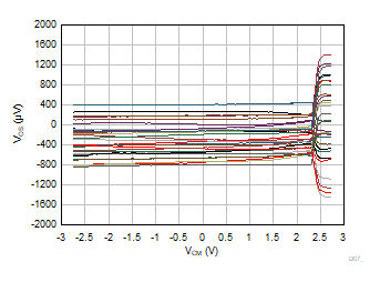
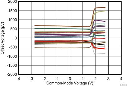
The input common-mode voltage range of the TLV904x series extends to either supply rails. This is true even when operating at the ultra-low supply voltage of 1.2 V, all the way up to the standard supply voltage of 5.5 V. This performance is achieved with a complementary input stage: an N-channel input differential pair in parallel with a P-channel differential pair. Refer to Section 8.2 for more details.
For most amplifiers with a complementary input stage, one of the input pairs, usually the P-channel input pair, is designed to deliver slightly better performance in terms of input offset voltage, offset drift over the N-channel pair. Consequently, the P-channel pair is designed to cover the majority of the common mode range with the N-channel pair slated to slowly take over at a certain threshold voltage from the positive rail. Just after the threshold voltage, both the input pairs are in operation for a small range referred to as the transition region. Beyond this region, the N-channel pair completely takes over. Within the transition region, PSRR, CMRR, offset voltage, offset drift, and THD can be degraded compared to device operation outside this region. Hence, most applications generally prefer operating in the P-channel input range where the performance is slightly better.
For the TLV904x, the P-channel pair is typically active for input voltages from the negative rail to (V+) – 0.4 V and the N-channel pair is typically active for input voltages from the positive supply to (V+) – 0.4 V. The transition region occurs typically from (V+) – 0.5 V to (V+) – 0.3 V, in which both pairs are on. These voltage levels mentioned above can vary with process variations associated with threshold voltage of transistors. In the TLV904x, 200-mV transition region mentioned above can vary up to 200 mV in either direction. Thus, the transition region (both stages on) can range from (V+) – 0.7 V to (V+) – 0.5 V on the low end, up to (V+) – 0.3 V to (V+) – 0.1 V on the high end.
Recollecting the fact that a P-channel input pair usually offers better performance over a N-channel input pair, the TLV904x is designed to offer a much wider P-channel input pair range, in comparison to most complimentary input amplifiers in the industry. A side by side comparison of the TLV904x and the TLV900x is provided below. Note, that the TLV900x guarantees P-channel pair operation only until 1.4 V from the positive rail while the TLV904x guarantees P-channel pair operation all the way till 0.7 V from the positive rail. This additional 700mV of P-channel input pair range for the TLV904x is particularly useful when operating at lower supply voltages (1.2 V, 1.8 V etc) where the P-channel input range usually gets limited to a great extent.
Thus the wide common mode swing of input signal can be accommodated more easily within the P-channel input pair of the TLV904x, while likely avoiding the transition region, thereby maintaining linearity.

| V+ = 2.75 V, V– = –2.75 V |

| V+ = 2.75 V, V– = –2.75 V |