JAJSIO2G March 2020 – March 2022 TLV9041 , TLV9042 , TLV9044
PRODUCTION DATA
- 1 特長
- 2 アプリケーション
- 3 概要
- 4 Revision History
- 5 Device Comparison Table
- 6 Pin Configuration and Functions
- 7 Specifications
-
8 Detailed Description
- 8.1 Overview
- 8.2 Functional Block Diagram
- 8.3
Feature Description
- 8.3.1 Operating Voltage
- 8.3.2 Rail-to-Rail Input
- 8.3.3 Rail-to-Rail Output
- 8.3.4 Common-Mode Rejection Ratio (CMRR)
- 8.3.5 Capacitive Load and Stability
- 8.3.6 Overload Recovery
- 8.3.7 EMI Rejection
- 8.3.8 Electrical Overstress
- 8.3.9 Input and ESD Protection
- 8.3.10 Shutdown Function
- 8.3.11 Packages With an Exposed Thermal Pad
- 8.4 Device Functional Modes
- 9 Application and Implementation
- 10Power Supply Recommendations
- 11Layout
- 12Device and Documentation Support
- 13Mechanical, Packaging, and Orderable Information
パッケージ・オプション
メカニカル・データ(パッケージ|ピン)
サーマルパッド・メカニカル・データ
- DPW|5
発注情報
8.3.9 Input and ESD Protection
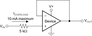
The TLV904x family incorporates internal ESD protection circuits on all pins. For input and output pins, this protection primarily consists of current-steering diodes connected between the input and power-supply pins. These ESD protection diodes provide in-circuit, input overdrive protection, as long as the current is limited to 10 mA. Figure 8-6 shows how a series input resistor can be added to the driven input to limit the input current. The added resistor contributes thermal noise at the amplifier input and the value must be kept to a minimum in noise-sensitive applications.
 Figure 8-6 Input Current Protection