JAJSLX4 May   2021 TMAG5123

PRODUCTION DATA  

  1. 特長
  2. アプリケーション
  3. 概要
  4. Revision History
  5. Device Comparison Table
  6. Pin Configuration and Functions
  7. Specifications
    1. 7.1 Absolute Maximum Ratings
    2. 7.2 ESD Ratings
    3. 7.3 Recommended Operating Conditions
    4. 7.4 Thermal Information
    5. 7.5 Electrical Characteristics
    6. 7.6 Magnetic Characteristics
    7. 7.7 Typical Characteristics
  8. Detailed Description
    1. 8.1 Overview
    2. 8.2 Functional Block Diagram
    3. 8.3 Feature Description
      1. 8.3.1 Field Direction Definition
      2. 8.3.2 Device Output
      3. 8.3.3 Protection Circuits
        1. 8.3.3.1 Load Dump Protection
        2. 8.3.3.2 Reverse Supply Protection
      4. 8.3.4 Hall Element Location
      5. 8.3.5 Power-On Time
      6. 8.3.6 Propagation Delay
      7. 8.3.7 Chopper Stabilization
    4. 8.4 Device Functional Modes
  9. Application and Implementation
    1. 9.1 Application Information
    2. 9.2 Typical Applications
      1. 9.2.1 In-Plane Typical Application Diagrams
        1. 9.2.1.1 Design Requirements
        2. 9.2.1.2 Detailed Design Procedure
        3. 9.2.1.3 Application Curve
  10. 10Power Supply Recommendations
  11. 11Layout
    1. 11.1 Layout Guidelines
    2. 11.2 Layout Example
  12. 12Device and Documentation Support
    1. 12.1 Receiving Notification of Documentation Updates
    2. 12.2 サポート・リソース
    3. 12.3 Trademarks
    4. 12.4 Electrostatic Discharge Caution
    5. 12.5 Glossary
  13. 13Mechanical, Packaging, and Orderable Information

パッケージ・オプション

メカニカル・データ(パッケージ|ピン)
サーマルパッド・メカニカル・データ
発注情報

Power-On Time

Figure 8-5 shows the behavior of the device after the VCC voltage is applied and when the field is below the BOP threshold. Once the minimum value for VCC is reached, the TMAG5123 will take time tON to power up and then time tPD to update the output to a level High.

Figure 8-6 shows the behavior of the device after the VCC voltage is applied and when the field is above the BOP threshold. Once the minimum value for VCC is reached, the TMAG5123 will take time tON to power up and then time tPD to update the output to a level Low.

The output value during tON is unknown in both cases. The output value at the end of tON will be set at High.
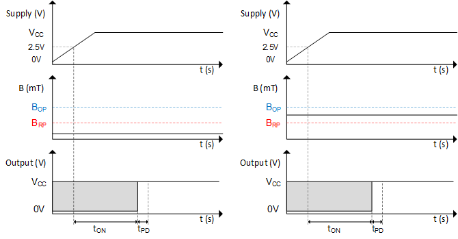
GUID-20201013-CA0I-XQBV-WC4V-QMFLLVB4G2S6-low.gif Figure 8-5 Power-On Time When B < BOP
GUID-20201013-CA0I-BBHT-Q3JT-9F6VXBR6HSC1-low.gif Figure 8-6 Power-On Time When B > BOP