JAJSJ71A June   2020  – December 2021 TMAG5170-Q1

PRODUCTION DATA  

  1. 特長
  2. アプリケーション
  3. 説明
  4. Revision History
  5. Pin Configuration and Functions
  6. Specifications
    1. 6.1 Absolute Maximum Ratings
    2. 6.2 ESD Ratings
    3. 6.3 Thermal Information
    4. 6.4 Recommended Operating Conditions
    5. 6.5 Electrical Characteristics
    6. 6.6 Magnetic Characteristics
    7. 6.7 Power up Timing
    8. 6.8 SPI Interface Timing
    9. 6.9 Typical Characteristics
  7. Detailed Description
    1. 7.1 Overview
    2. 7.2 Functional Block Diagram
    3. 7.3 Feature Description
      1. 7.3.1 Magnetic Flux Direction
      2. 7.3.2 Sensor Location
      3. 7.3.3 Magnetic Range Selection
      4. 7.3.4 Update Rate Settings
      5. 7.3.5 ALERT Function
        1. 7.3.5.1 Interrupt and Trigger Mode
        2. 7.3.5.2 Magnetic Switch Mode
      6. 7.3.6 Threshold Count
      7. 7.3.7 Diagnostics
        1. 7.3.7.1  Memory CRC Check
        2. 7.3.7.2  ALERT Integrity Check
        3. 7.3.7.3  VCC Check
        4. 7.3.7.4  Internal LDO Under Voltage Check
        5. 7.3.7.5  Digital Core Power-on Reset Check
        6. 7.3.7.6  SDO Output Check
        7. 7.3.7.7  Communication CRC Check
        8. 7.3.7.8  Oscillator Integrity Check
        9. 7.3.7.9  Magnetic Field Threshold Check
        10. 7.3.7.10 Temperature Alert Check
        11. 7.3.7.11 Analog Front-End (AFE) Check
        12. 7.3.7.12 Hall Resistance and Switch Matrix Check
        13. 7.3.7.13 Hall Offset Check
        14. 7.3.7.14 ADC Check
    4. 7.4 Device Functional Modes
      1. 7.4.1 Operating Modes
        1. 7.4.1.1 Active Mode
        2. 7.4.1.2 Standby Mode
        3. 7.4.1.3 Configuration Mode (DEFAULT)
        4. 7.4.1.4 Sleep Mode
        5. 7.4.1.5 Wake-Up and Sleep Mode
        6. 7.4.1.6 Deep-Sleep Mode
    5. 7.5 Programming
      1. 7.5.1 Data Definition
        1. 7.5.1.1 Magnetic Sensor Data
        2. 7.5.1.2 Temperature Sensor Data
        3. 7.5.1.3 Magnetic Sensor Offset Correction
        4. 7.5.1.4 Angle and Magnitude Data Definition
      2. 7.5.2 SPI Interface
        1. 7.5.2.1 SCK
        2. 7.5.2.2 CS
        3. 7.5.2.3 SDI
        4. 7.5.2.4 SDO
          1. 7.5.2.4.1 Regular 32-Bit SDO Read
          2. 7.5.2.4.2 Special 32-Bit SDO Read
        5. 7.5.2.5 SPI CRC
        6. 7.5.2.6 SPI Frame
          1. 7.5.2.6.1 32-Bit Read Frame
          2. 7.5.2.6.2 32-Bit Write Frame
    6. 7.6 Register Map
      1. 7.6.1 TMAG5170 Registers
  8. Application and Implementation
    1. 8.1 Application Information
      1. 8.1.1 Selecting the Sensitivity Option
      2. 8.1.2 Temperature Compensation for Magnets
      3. 8.1.3 Sensor Conversion
        1. 8.1.3.1 Continuous Conversion
        2. 8.1.3.2 Trigger Conversion
        3. 8.1.3.3 Pseudo-Simultaneous Sampling
      4. 8.1.4 Error Calculation During Linear Measurement
      5. 8.1.5 Error Calculation During Angular Measurement
    2. 8.2 Typical Application
      1. 8.2.1 Design Requirements
        1. 8.2.1.1 Gain Adjustment for Angle Measurement
      2. 8.2.2 Detailed Design Procedure
      3. 8.2.3 Application Curves
    3. 8.3 Do's and Don'ts
  9. Power Supply Recommendations
  10. 10Layout
    1. 10.1 Layout Guidelines
    2. 10.2 Layout Example
  11. 11Device and Documentation Support
    1. 11.1 Receiving Notification of Documentation Updates
    2. 11.2 サポート・リソース
    3. 11.3 Trademarks
    4. 11.4 Electrostatic Discharge Caution
    5. 11.5 Glossary
  12. 12Mechanical, Packaging, and Orderable Information

パッケージ・オプション

メカニカル・データ(パッケージ|ピン)
サーマルパッド・メカニカル・データ
発注情報

Temperature Sensor Data

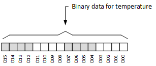
The TMAG5170-Q1 temperature sensor will measure temperature from –40°C to 170°C. Figure 7-6 shows the temperature stored in the 16-bit TEMP_RESULT register. With DATA_TYPE = 00b, the 16-bit temperature data can be accessed through regular 32-bit SPI read. Use Equation 15 to calculate the temperature.

Equation 3. GUID-8EF8C240-8B0B-4640-8597-184D0B35CC15-low.gif

where

  • T is the measured temperature in degree Celsius.
  • TSENS_T0 is the reference temperature in degree Celsius as listed in the Section 6.5 table.
  • TADCRES is the change in ADC code per degree Celsius as listed in the Section 6.5 table.
  • TADCT0 is the TEMP_RESULT decimal value at reference temperature, TSENS_T0 as listed in the Section 6.5 table.
  • TADCT is the measured TEMP_RESULT decimal value for temperature T.

With DATA_TYPE ≠ 00b, the 12 MSB bits from the TEMP_RESULT register can be accessed. In this mode, use Equation 17 to calculate the temperature.

Equation 4. GUID-648BF42C-C867-4042-8DF8-3C594374675B-low.gif
GUID-9A491250-017F-452C-BEB7-4D9F1A9F3AFA-low.gifFigure 7-6 Temperature Sensor Data Definition