JAJSH90D April   2019  – June 2022 TMP235-Q1 , TMP236-Q1

PRODUCTION DATA  

  1. 特長
  2. アプリケーション
  3. 概要
  4. Revision History
  5. Pin Configuration and Functions
  6. Specifications
    1. 6.1 Absolute Maximum Ratings
    2. 6.2 ESD Ratings
    3. 6.3 Recommended Operating Conditions
    4. 6.4 Thermal Information
    5. 6.5 Electrical Characteristics
    6. 6.6 Typical Characteristics
  7. Detailed Description
    1. 7.1 Overview
    2. 7.2 Functional Block Diagram
    3. 7.3 Feature Description
    4. 7.4 Device Functional Modes
  8. Application and Implementation
    1. 8.1 Application Information
    2. 8.2 Typical Application
      1. 8.2.1 Connection to an ADC
        1. 8.2.1.1 Design Requirements
        2. 8.2.1.2 Detailed Design Procedure
        3. 8.2.1.3 Application Curve
  9. Power Supply Recommendations
  10. 10Layout
    1. 10.1 Layout Guidelines
    2. 10.2 Layout Examples
  11. 11Device and Documentation Support
    1. 11.1 Receiving Notification of Documentation Updates
    2. 11.2 サポート・リソース
    3. 11.3 Trademarks
    4. 11.4 Electrostatic Discharge Caution
    5. 11.5 Glossary
  12. 12Mechanical, Packaging, and Orderable Information

パッケージ・オプション

メカニカル・データ(パッケージ|ピン)
サーマルパッド・メカニカル・データ
発注情報

Typical Characteristics

at TA = 25°C, (unless otherwise noted)
GUID-43460414-9EC2-4705-AF96-8781677A2C89-low.gif
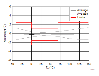
TMP235-Q1: VDD = 2.3 to 5.5 V, IOUT = 0 µA, CLOAD = 1000 pF
Figure 6-1 Accuracy vs TA Temperature
GUID-EA0367ED-517D-4301-91E3-E4DFBB7DF758-low.gif
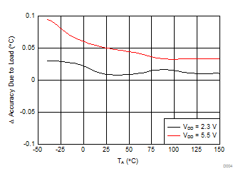
TMP23x-Q1: IOUT = from 0 µA to 100 µA, CLOAD = 1000 pF
Figure 6-3 Changes in Accuracy vs Ambient Temperature (Due to Load)
GUID-E16DD7BC-893F-49DC-8FF6-77D38EA7AD38-low.gif
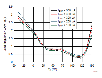
TMP23x-Q1: VDD = 2.3 V, CLOAD = 1000 pF
Figure 6-5 Load Regulation vs Ambient Temperature
GUID-7093A9C0-2EA0-4EB7-8DEF-0A228A26EDBD-low.gif
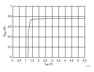
TMP23x-Q1: TA = 25°C
Figure 6-7 Output Voltage vs Power Supply
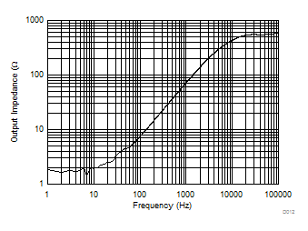
GUID-052C4682-083A-4CD1-915A-D6CD183A15EC-low.gif
TMP23x-Q1: TA = 25°C, VDD = 5 V, IOUT = 100 µA
Figure 6-9 Output Impedance vs Frequency
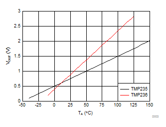
GUID-1D8250A7-1E6F-43A4-A6E8-944C956BBC4D-low.gif
IOUT = 0 µA, CLOAD = 1000 pF
Figure 6-2 Output Voltage vs Ambient Temperature
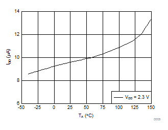
GUID-22DF8684-3EEF-4694-A028-E813AAE9153E-low.gif
TMP23x-Q1: IOUT = 0 µA, CLOAD = 1000 pF
Figure 6-4 Supply Current vs Temperature
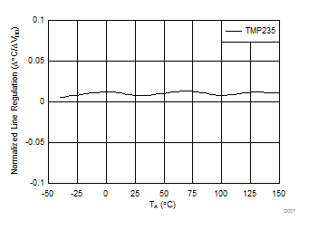
GUID-060FDA7A-5EBE-45CA-B408-5A1EE98E3545-low.gif
TMP23x-Q1: VDD = 2.3 to 5.5 V, IOUT = 0 µA, CLOAD = 1000 pF
Figure 6-6 Line Regulation (Δ°C / ΔVDD) vs Ambient Temperature
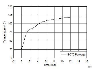
GUID-39734B23-AFE0-4E9D-B84A-8942FE96E34A-low.gif
TMP23x-Q1: 1 × 1 (inches) PCB, Air 26°C to Fluid Bath 123°C
Figure 6-8 Thermal Response (Air-to-Fluid Bath)