JAJSG54A September   2018  – December 2018 TMUX1511

PRODUCTION DATA.  

  1. 特長
  2. アプリケーション
  3. 概要
    1.     Device Images
      1.      アプリケーションの例
      2.      ブロック図
  4. 改訂履歴
  5. Pin Configuration and Functions
    1.     Pin Functions
  6. Specifications
    1. 6.1 Absolute Maximum Ratings
    2. 6.2 ESD Ratings
    3. 6.3 Recommended Operating Conditions
    4. 6.4 Thermal Information
    5. 6.5 Electrical Characteristics
    6. 6.6 Dynamic Characteristics
    7. 6.7 Timing Requirements
    8. 6.8 Typical Characteristics
      1. 6.8.1 Eye Diagrams
  7. Parameter Measurement Information
    1. 7.1  On-Resistance
    2. 7.2  Off-Leakage Current
    3. 7.3  On-Leakage Current
    4. 7.4  IPOFF Leakage Current
    5. 7.5  Transition Time
    6. 7.6  TON (VDD) and TOFF (VDD) Time
    7. 7.7  Propagation Delay
    8. 7.8  Skew
    9. 7.9  Charge Injection
    10. 7.10 Capacitance
    11. 7.11 Off Isolation
    12. 7.12 Channel-to-Channel Crosstalk
    13. 7.13 Bandwidth
  8. Detailed Description
    1. 8.1 Overview
    2. 8.2 Functional Block Diagram
    3. 8.3 Feature Description
      1. 8.3.1 Bidirectional Operation
      2. 8.3.2 Beyond Supply Operation
      3. 8.3.3 1.8 V Logic Compatible Inputs
      4. 8.3.4 Powered-off Protection
      5. 8.3.5 Fail-Safe Logic
      6. 8.3.6 Low Capacitance
      7. 8.3.7 Integrated Pull-Down Resistors
    4. 8.4 Device Functional Modes
    5. 8.5 Truth Tables
  9. Application and Implementation
    1. 9.1 Application Information
    2. 9.2 Typical Application
      1. 9.2.1 Protocol / Signal Isolation
        1. 9.2.1.1 Design Requirements
        2. 9.2.1.2 Detailed Design Procedure
        3. 9.2.1.3 Application Curves
      2. 9.2.2 Transimpedance Amplifier Feedback Control
        1. 9.2.2.1 Design Requirements
        2. 9.2.2.2 Detailed Design Procedure
        3. 9.2.2.3 Application Curves
  10. 10Power Supply Recommendations
  11. 11Layout
    1. 11.1 Layout Guidelines
    2. 11.2 Layout Example
  12. 12デバイスおよびドキュメントのサポート
    1. 12.1 ドキュメントのサポート
      1. 12.1.1 関連資料
    2. 12.2 ドキュメントの更新通知を受け取る方法
    3. 12.3 コミュニティ・リソース
    4. 12.4 商標
    5. 12.5 静電気放電に関する注意事項
    6. 12.6 Glossary
  13. 13メカニカル、パッケージ、および注文情報

パッケージ・オプション

メカニカル・データ(パッケージ|ピン)
サーマルパッド・メカニカル・データ
発注情報

Transimpedance Amplifier Feedback Control

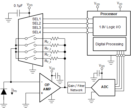
Switches and multiplexers are commonly used in the feedback path of amplifier circuits to provide configurable gain control. By using various resistor values on each switch path the TMUX1511 allows the system to have multiple gain settings. An external resistor, or utilizing 1 channel always being closed, ensures the amplifier isn't operating in an open loop configuration. A transimpedance amplifier (TIA) for photodiodes is a common circuit that requires gain control using a multi-channel switch to convert the output current of the photodiode into a voltage for the MCU or processor. The leakage current, capacitance, and charge injection performance of the TMUX1511 are key specifications to evaluate when selecting a device for gain control.
TMUX1511 Typical-Application-Analog.gifFigure 42. Multiplexing Gain for a TIA Circuit