JAJSG83A September 2018 – December 2018 TMUX6119
PRODUCTION DATA.
- 1 特長
- 2 アプリケーション
- 3 概要
- 4 改訂履歴
- 5 Pin Configuration and Functions
-
6 Specifications
- 6.1 Absolute Maximum Ratings
- 6.2 ESD Ratings
- 6.3 Thermal Information
- 6.4 Recommended Operating Conditions
- 6.5 Electrical Characteristics (Dual Supplies: ±15 V)
- 6.6 Switching Characteristics (Dual Supplies: ±15 V)
- 6.7 Electrical Characteristics (Single Supply: 12 V)
- 6.8 Switching Characteristics (Single Supply: 12 V)
- 6.9 Typical Characteristics
- 7 Parameter Measurement Information
-
8 Detailed Description
- 8.1
Overview
- 8.1.1 On-Resistance
- 8.1.2 Off-Leakage Current
- 8.1.3 On-Leakage Current
- 8.1.4 Transition Time
- 8.1.5 Break-Before-Make Delay
- 8.1.6 Enable Turn-On and Enable Turn-Off Time
- 8.1.7 Charge Injection
- 8.1.8 Off Isolation
- 8.1.9 Channel-to-Channel Crosstalk
- 8.1.10 Bandwidth
- 8.1.11 THD + Noise
- 8.1.12 AC Power Supply Rejection Ratio (AC PSRR)
- 8.2 Functional Block Diagram
- 8.3 Feature Description
- 8.4 Device Functional Modes
- 8.1
Overview
- 9 Application and Implementation
- 10Power Supply Recommendations
- 11Layout
- 12デバイスおよびドキュメントのサポート
- 13メカニカル、パッケージ、および注文情報
9.2.3 Application Curve
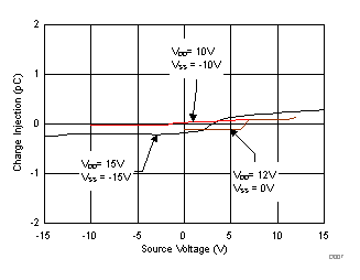
Fast transition time and small charge injection are two critical parameters for the SPDT switches used in the chopper amplifier design. Figure 35 shows the plot for the charge injection vs. source voltage for the TMUX6119.
 Figure 35. Charge Injection vs Source Voltage