JAJSKW6 december 2020 TMUXHS4412
PRODUCTION DATA
- 1
- 1 特長
- 2 アプリケーション
- 3 概要
- 4 Revision History
- 5 Pin Configuration and Functions
- 6 Specifications
- 7 Detailed Description
- 8 Application and Implementation
- 9 Power Supply Recommendations
- 10Layout
- 11Device and Documentation Support
- 12Mechanical, Packaging, and Orderable Information
パッケージ・オプション
メカニカル・データ(パッケージ|ピン)
- RUA|42
サーマルパッド・メカニカル・データ
- RUA|42
発注情報
6.8 Typical Characteristics
Figure 6-1 shows differential insertion loss on the top plot and return loss on the bottom plot of a
typical TMUXHS4412 channel. Note measurements are performed in TI evaluation board with
board and equipment parasitics calibrated out.
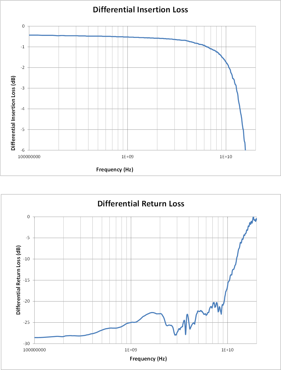 Figure 6-1 S-parameter plots for a TMUXHS4412
channel - top: differential insertion loss, and bottom: return loss vs frequency
 Figure 6-1 S-parameter plots for a TMUXHS4412
channel - top: differential insertion loss, and bottom: return loss vs frequency
Figure 6-1 S-parameter plots for a TMUXHS4412
channel - top: differential insertion loss, and bottom: return loss vs frequencyFigure 6-2 shows side by side comparison of 10 Gbps signals through calibration traces and a typical
TMUXHS4412 channels.
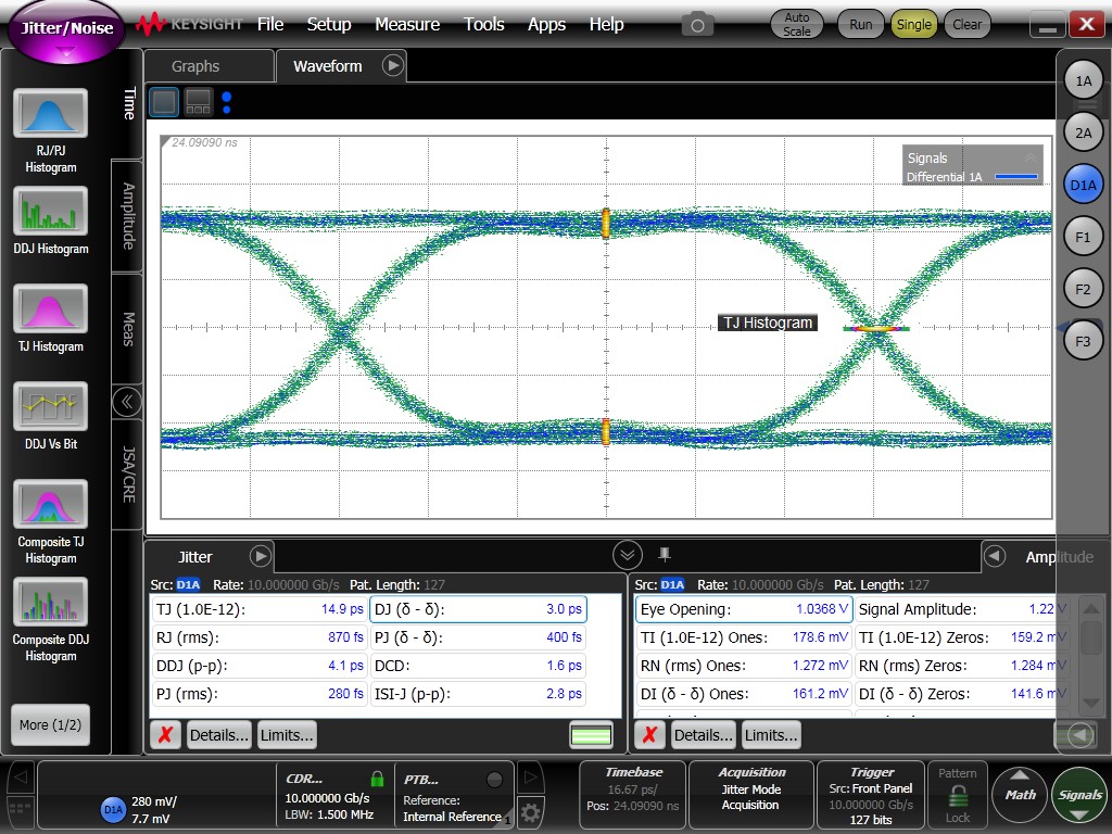
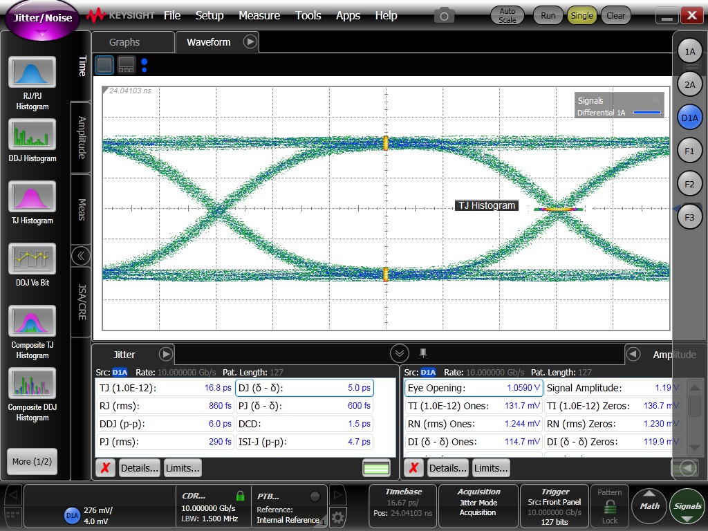 Figure 6-2 Jitter decomposition of 10
Gbps PRBS-7 signals in TI evaluation board - Top: through calibration
traces, Bottom: through a typical TMUXHS4412 channels

 Figure 6-2 Jitter decomposition of 10
Gbps PRBS-7 signals in TI evaluation board - Top: through calibration
traces, Bottom: through a typical TMUXHS4412 channels
Figure 6-3 shows side by side comparison of 20 Gbps signals through calibration traces and a typical
TMUXHS4412 channels.
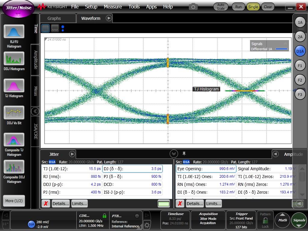
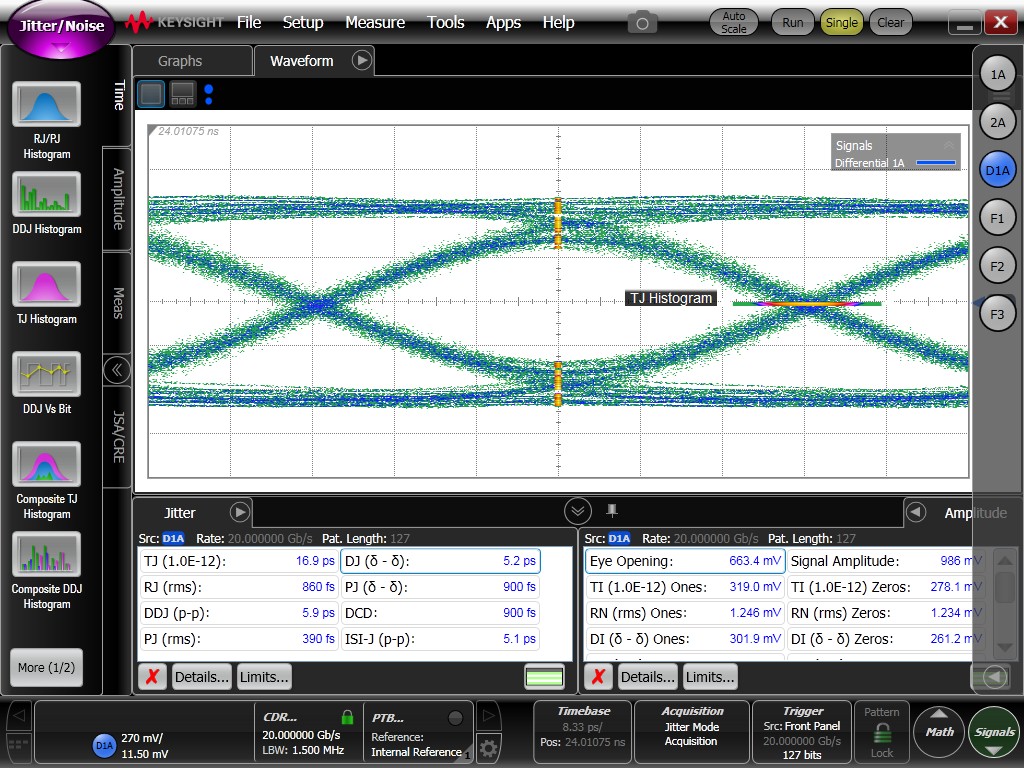 Figure 6-3 Jitter
decomposition of 20 Gbps PRBS-7 signals in TI evaluation board - Top: through
calibration traces, Bottom: through a typical TMUXHS4412 channels

 Figure 6-3 Jitter
decomposition of 20 Gbps PRBS-7 signals in TI evaluation board - Top: through
calibration traces, Bottom: through a typical TMUXHS4412 channels