SLVSC54B July 2013 – April 2014 TPD4E110
PRODUCTION DATA.
- 1 Features
- 2 Applications
- 3 Description
- 4 Simplified Schematic
- 5 Revision History
- 6 Terminal Configuration and Functions
- 7 Specifications
- 8 Detailed Description
- 9 Applications and Implementation
- 10Layout
- 11Device and Documentation Support
- 12Mechanical, Packaging, and Orderable Information
パッケージ・オプション
メカニカル・データ(パッケージ|ピン)
- DPW|4
サーマルパッド・メカニカル・データ
- DPW|4
発注情報
7 Specifications
7.1 Absolute Maximum Ratings(1)
over operating free-air temperature range (unless otherwise noted)| MIN | MAX | UNIT | ||
|---|---|---|---|---|
| Operating temperature range | -40 | 125 | °C | |
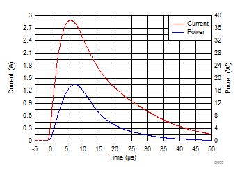
| IPP | Peak pulse current (tp = 8/20μs) | 2.5 | A | |
| PPP(forward) | Peak pulse power (tp = 8/20μs) | 35 | W | |
| PPP(reverse) | Peak pulse power (tp = 8/20μs) | 18 | W |
(1) Stresses beyond those listed under absolute maximum ratings may cause permanent damage to the device. These are stress ratings only, and functional operation of the device at these or any other conditions beyond those indicated under recommended operating conditions is not implied. Exposure to absolute-maximum-rated conditions for extended periods may affect device reliability.
7.2 Handling Ratings
| MIN | MAX | UNIT | ||
|---|---|---|---|---|
| Tstg | Storage temperature | –65 | 155 | °C |
| ESD(1) | IEC 61000-4-2 contact ESD | ±12 | kV | |
| IEC 61000-4-2 air-gap ESD | ±15 | kV | ||
(1) Electrostatic discharge (ESD) to measure device sensitivity and immunity to damage caused by assembly line electrostatic discharges in to the device.
7.3 Recommended Operating Conditions
over operating free-air temperature range (unless otherwise noted)| MIN | MAX | UNIT | ||
|---|---|---|---|---|
| VIO | 0.0 | 5.5 | V | |
| TA | Operating free-air temperature | –40 | 125 | °C |
7.4 Thermal Information
| THERMAL METRIC(1) | TPD4E110 | UNIT | |
|---|---|---|---|
| DPW (4 TERMINALS) |
|||
| RθJA | Junction-to-ambient thermal resistance | 291.8 | °C/W |
| RθJC(top) | Junction-to-case (top) thermal resistance | 224.2 | |
| RθJB | Junction-to-board thermal resistance | 245.8 | |
| ψJT | Junction-to-top characterization parameter | 31.4 | |
| ψJB | Junction-to-board characterization parameter | 245.6 | |
| RθJC(bot) | Junction-to-case (bottom) thermal resistance | 195.4 | |
(1) For more information about traditional and new thermal metrics, see the IC Package Thermal Metrics application report, SPRA953.
7.5 Electrical Characteristics
TA = 25°C (unless otherwise noted)| PARAMETER | TEST CONDITION | MIN | TYP | MAX | UNIT | |
|---|---|---|---|---|---|---|
| VRWM | Reverse stand-off voltage | IIO = 10 μA | 5.5 | V | ||
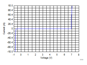
| VCLAMP | Clamp voltage with ESD strike | I = 1A, TLP, I/O to GND | 10 | V | ||
| I = 5A, TLP, I/O to GND | 13 | V | ||||
| I = 1A, TLP, GND to I/O | 3 | V | ||||
| I = 5A, TLP, GND to I/O | 6 | V | ||||
| VBR | Break-down voltage | IIO = 1mA | 6.5 | 7.5 | 8.5 | V |
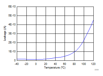
| ILEAK | Leakage current | VIO = 2.5V | 0.02 | 1 | nA | |
| RDYN | Dynamic resistance | Any I/O to GND Terminal(1) | 0.8 | Ω | ||
| GND to any I/O Terminal(1) | 0.7 | Ω | ||||
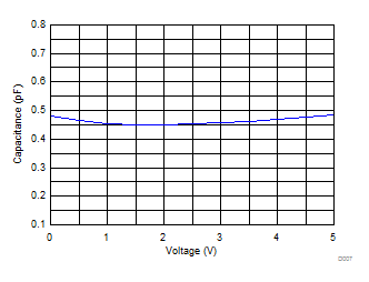
| CL | Line capacitance | VIO = 2.5V, f = 1MHz, I/O to GND | 0.45 | 0.55 | pF | |
| CCROSS | Channel to channel input capacitance | GND Terminal = 0V, f = 1MHz, VBIAS = 2.5 V, between channel terminals |
0.003 | pF | ||
| ΔCIO-TO-GND | Variation of channel input capacitance | GND Terminal = 0V, f = 1MHz, VBIAS = 2.5 V, Channel_x terminal to GND – Channel_y terminal to GND |
0.05 | pF | ||
(1) Extraction of RDYN using least squares fit of TLP characteristics between I = 10A and I = 20A.
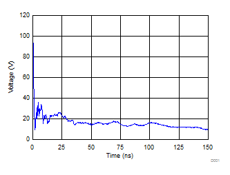
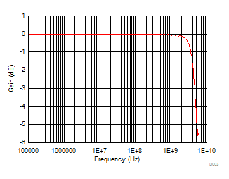
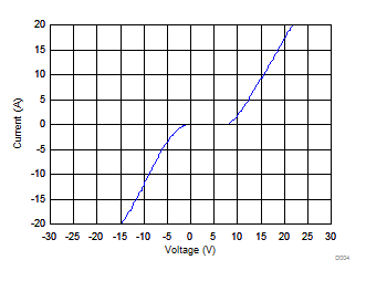
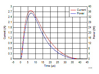
7.6 Typical Characteristics
At TA = 25°C, unless otherwise noted