SLVSBQ9D December   2012  – April 2017 TPD4E1U06

PRODUCTION DATA.  

  1. Features
  2. Applications
  3. Description
  4. Revision History
  5. Pin Configuration and Functions
  6. Specifications
    1. 6.1 Absolute Maximum Ratings
    2. 6.2 ESD Ratings
    3. 6.3 ESD Ratings—IEC Specification
    4. 6.4 Recommended Operating Conditions
    5. 6.5 Thermal Information
    6. 6.6 Electrical Characteristics
    7. 6.7 Typical Characteristics
  7. Detailed Description
    1. 7.1 Overview
    2. 7.2 Functional Block Diagram
    3. 7.3 Feature Description
      1. 7.3.1 IEC 61000-4-2 Level 4 ESD Protection
      2. 7.3.2 IEC 61000-4-5 Surge Protection
      3. 7.3.3 IEC 61000-4-4 EFT Protection
      4. 7.3.4 IO Capacitance
      5. 7.3.5 DC Breakdown Voltage
      6. 7.3.6 Ultra Low Leakage Current
      7. 7.3.7 Low ESD Clamping Voltage
      8. 7.3.8 Industrial Temperature Range
      9. 7.3.9 Small, Easy-to-Route Packages
    4. 7.4 Device Functional Modes
  8. Application and Implementation
    1. 8.1 Application Information
    2. 8.2 Typical Application
      1. 8.2.1 Design Requirements
      2. 8.2.2 Detailed Design Procedure
        1. 8.2.2.1 Signal Range on Pins 1, 3, 4, or 6
        2. 8.2.2.2 Operating Frequency
      3. 8.2.3 Application Curve
  9. Power Supply Recommendations
  10. 10Layout
    1. 10.1 Layout Guidelines
    2. 10.2 Layout Example
  11. 11Device and Documentation Support
    1. 11.1 Documentation Support
      1. 11.1.1 Related Documentation
    2. 11.2 Receiving Notification of Documentation Updates
    3. 11.3 Community Resources
    4. 11.4 Trademarks
    5. 11.5 Electrostatic Discharge Caution
    6. 11.6 Glossary
  12. 12Mechanical, Packaging, and Orderable Information

パッケージ・オプション

メカニカル・データ(パッケージ|ピン)
サーマルパッド・メカニカル・データ
発注情報

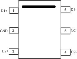
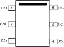
Pin Configuration and Functions

DCK Package
6-Pin SC70
Top View
TPD4E1U06 DCK_SLVSBQ9.gif
DBV Package
6-Pin SOT-23
Top View
TPD4E1U06 DBV_SLVSBQ9.gif

Pin Functions

PIN I/O DESCRIPTION
NAME NO.
D1+ 1 I/O ESD protected channel. Connect to data line as close to the connector as possible
D1– 6 I/O
D2– 4 I/O
D2+ 3 I/O
GND 2 GND Ground. Connect to ground
NC 5 I/O No connect. Can be left floating, grounded, or connected to VCC