SLVSB49F November 2011 – January 2015 TPS22910A , TPS22912C
PRODUCTION DATA.
- 1 Features
- 2 Applications
- 3 Description
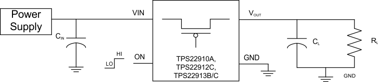
- 4 Simplified Schematic
- 5 Revision History
- 6 Device Comparison Table
- 7 Pin Configuration and Functions
-
8 Specifications
- 8.1 Absolute Maximum Ratings
- 8.2 ESD Ratings
- 8.3 Recommended Operating Conditions
- 8.4 Thermal Information
- 8.5 Electrical Characteristics
- 8.6 Switching Characteristics, Typical
- 8.7 Typical DC Characteristics
- 8.8 Typical AC Characteristics, TPS22910A
- 8.9 Typical AC Characteristics, TPS22912C
- 8.10 Typical AC Characteristics, TPS22913B
- 8.11 Typical AC Characteristics, TPS22913C
- 9 Parameter Measurement Information
- 10Detailed Description
- 11Application and Implementation
- 12Power Supply Recommendations
- 13Layout
- 14Device and Documentation Support
- 15Mechanical, Packaging, and Orderable Information
1 Features
- Integrated Single Load Switch
- Four Pin Wafer-Chip-Scale Package (Nom)
- 0.9 mm × 0.9 mm, 0.5-mm Pitch, 0.5-mm Height (YZV)
- Input Voltage Range: 1.4 V to 5.5 V
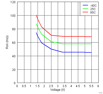
- Low ON-Resistance
- rON = 60 mΩ at VIN = 5 V
- rON = 61 mΩ at VIN = 3.3 V
- rON = 74 mΩ at VIN = 1.8 V
- rON = 84 mΩ at VIN = 1.5 V
- 2-A Maximum Continuous Switch Current
- Low Threshold Control Input
- Controlled Slew-rate
- Under-Voltage Lock Out
- Full-Time Reverse Current Protection
- Quick Output Discharge Transistor (TPS22913B/C Devices)
2 Applications
- Notebook Computer and Ultrabook™
- Tablets and Set-Top-Boxes
- Portable Industrial / Medical Equipment
- Portable Media Players
- Point Of Sale Pins
- GPS Navigation Devices
- Digital Cameras
- Portable Instrumentation
- Smartphones / Wireless Handsets
3 Description
The TPS22910A, TPS22912C, and TPS22913B/C are small, low rON load switches with controlled turn on. The device contains a P-channel MOSFET that can operate over an input voltage range of 1.4 V to 5.5 V. The switch is controlled by an on/off input (ON), which is capable of interfacing directly with low-voltage GPIO control signals.
The TPS22910A, TPS22912C, and TPS22913B/C devices provide reverse current protection in ON and OFF states. An internal reverse voltage comparator disables the power-switch when the output voltage (VOUT) is driven higher than the input voltage (VIN), by VRCP, to quickly (10 µs typ) stop the flow of current towards the input side of the switch. Reverse current protection is always active, even when the power-switch is disabled. Additionally, under-voltage lockout (UVLO) protection turns the switch off if the input voltage is too low.
The TPS22913B/C contains a 150-Ω on-chip load resistor for quick output discharge when the switch is turned off.
This family of devices have various slew rate options to avoid inrush current (see Device Comparison Table for details), are available in an ultra-small, space-saving 4-pin WCSP packages, and are characterized for operation over the free-air temperature range of –40°C to 85°C.
Device Information(1)
| PART NUMBER | PACKAGE | BODY SIZE (NOM) |
|---|---|---|
| TPS22910A | DSBGA (4) | 0.90 mm × 0.90 mm |
| TPS22912C | ||
| TPS22913B | ||
| TPS22913C |
- For all available packages, see the orderable addendum at the end of the datasheet.
4 Simplified Schematic
On-State Resistance vs Input Voltage