JAJSIO9E March   2014  – June 2021 TPS25200

PRODUCTION DATA  

  1. 特長
  2. アプリケーション
  3. 概要
  4. Revision History
  5. Pin Configuration and Functions
  6. Specifications
    1. 6.1 Absolute Maximum Ratings
    2. 6.2 ESD Ratings
    3. 6.3 Recommended Operating Conditions
    4. 6.4 Thermal Information
    5. 6.5 Electrical Characteristics
    6. 6.6 Timing Requirements
    7. 6.7 Typical Characteristics
  7. Parameter Measurement Information
  8. Detailed Description
    1. 8.1 Overview
    2. 8.2 Functional Block Diagram
    3. 8.3 Feature Description
      1. 8.3.1 Enable
      2. 8.3.2 Thermal Sense
      3. 8.3.3 Overcurrent Protection
      4. 8.3.4 FAULT Response
      5. 8.3.5 Output Discharge
    4. 8.4 Device Functional Modes
      1. 8.4.1 Undervoltage Lockout (UVLO)
      2. 8.4.2 Overcurrent Protection (OCP)
      3. 8.4.3 Overvoltage Clamp (OVC)
      4. 8.4.4 Overvoltage Lockout (OVLO)
  9. Application and Implementation
    1. 9.1 Application Information
    2. 9.2 Typical Application
      1. 9.2.1 Design Requirements
      2. 9.2.2 Detailed Design Procedure
        1. 9.2.2.1 Step by Step Design Produce
        2. 9.2.2.2 Input and Output Capacitance
        3. 9.2.2.3 Programming the Current-Limit Threshold
        4. 9.2.2.4 Design Above a Minimum Current Limit
        5. 9.2.2.5 Design Below a Maximum Current Limit
        6. 9.2.2.6 Power Dissipation and Junction Temperature
      3. 9.2.3 Application Curves
  10. 10Power Supply Recommendations
  11. 11Layout
    1. 11.1 Layout Guidelines
    2. 11.2 Layout Example
  12. 12Device and Documentation Support
    1. 12.1 Documentation Support
      1. 12.1.1 Related Documentation
    2. 12.2 Receiving Notification of Documentation Updates
    3. 12.3 サポート・リソース
    4. 12.4 Trademarks
    5. 12.5 Electrostatic Discharge Caution
    6. 12.6 Glossary
  13. 13Mechanical, Packaging, and Orderable Information

パッケージ・オプション

メカニカル・データ(パッケージ|ピン)
サーマルパッド・メカニカル・データ
発注情報

Input and Output Capacitance

Input and output capacitance improves the performance of the device; the actual capacitance must be optimized for the particular application. For all applications, a 0.1-µF or greater ceramic bypass capacitor between IN and GND is recommended as close to the device as possible for local noise decoupling.

When VIN ramp up exceed 7.6 V, VOUT follows VIN until the TPS25200 turns off the internal MOSFET after t(OVLO_off_delay). Since t(OVLO_off_delay) largely depends on the VIN ramp rate, VOUT sees some peak voltage. Increasing the output capacitance can lower the output peak voltage as shown in Figure 9-3.
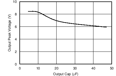
GUID-BBB3D60E-3A20-4DAF-BFC7-241FF2B31800-low.pngFigure 9-3 VOUT Peak Voltage vs COUT (VIN Step From 5 V to 15 V with 1-V/µs Ramp Up Rate)