JAJSJU4D May   2020  – September 2021 TPS25850-Q1 , TPS25851-Q1 , TPS25852-Q1

PRODUCTION DATA  

  1. 特長
  2. アプリケーション
  3. 概要
  4. Revision History
  5. 概要 (続き)
  6. Device Comparison Table
  7. Pin Configuration and Functions
  8. Specifications
    1. 8.1 Absolute Maximum Ratings
    2. 8.2 ESD Ratings
    3. 8.3 Recommended Operating Conditions
    4. 8.4 Thermal Information
    5. 8.5 Electrical Characteristics
    6. 8.6 Timing Requirements
    7. 8.7 Switching Characteristics
    8. 8.8 Typical Characteristics
  9. Parameter Measurement Information
  10. 10Detailed Description
    1. 10.1 Overview
    2. 10.2 Functional Block Diagram
    3. 10.3 Feature Description
      1. 10.3.1  Power-Down or Undervoltage Lockout
      2. 10.3.2  Input Overvoltage Protection (OVP) - Continuously Monitored
      3. 10.3.3  Buck Converter
      4. 10.3.4  FREQ/SYNC
      5. 10.3.5  Bootstrap Voltage (BOOT)
      6. 10.3.6  Minimum ON-Time, Minimum OFF-Time
      7. 10.3.7  Internal Compensation
      8. 10.3.8  Selectable Output Voltage (VSET)
      9. 10.3.9  Current Limit and Short Circuit Protection
        1. 10.3.9.1 USB Switch Programmable Current Limit (ILIM)
        2. 10.3.9.2 Interlocking for Two-Level USB Switch Current Limit
        3. 10.3.9.3 Cycle-by-Cycle Buck Current Limit
        4. 10.3.9.4 OUT Current Limit
      10. 10.3.10 Cable Compensation
      11. 10.3.11 Thermal Management With Temperature Sensing (TS) and OTSD
      12. 10.3.12 Thermal Shutdown
      13. 10.3.13 USB Enable On/Off Control (TPS25852-Q1)
      14. 10.3.14 FAULT Indication (TPS25851-Q1 and TPS25852-Q1)
      15. 10.3.15 USB Specification Overview
      16. 10.3.16 USB Type-C® Basics
        1. 10.3.16.1 Configuration Channel
        2. 10.3.16.2 Detecting a Connection
        3. 10.3.16.3 Plug Polarity Detection (TPS25851-Q1)
      17. 10.3.17 USB Port Operating Modes
        1. 10.3.17.1 USB Type-C® Mode
        2. 10.3.17.2 Dedicated Charging Port (DCP) Mode (TPS25850-Q1 Only)
          1. 10.3.17.2.1 DCP BC1.2 and YD/T 1591-2009
          2. 10.3.17.2.2 DCP Divider-Charging Scheme
          3. 10.3.17.2.3 DCP 1.2-V Charging Scheme
        3. 10.3.17.3 DCP Auto Mode (TPS25850-Q1)
    4. 10.4 Device Functional Modes
      1. 10.4.1 Shutdown Mode
      2. 10.4.2 Active Mode
  11. 11Application and Implementation
    1. 11.1 Application Information
    2. 11.2 Typical Applications
      1. 11.2.1 Design Requirements
      2. 11.2.2 Detailed Design Procedure
        1. 11.2.2.1 Output Voltage Setting
        2. 11.2.2.2 Switching Frequency
        3. 11.2.2.3 Inductor Selection
        4. 11.2.2.4 Output Capacitor Selection
        5. 11.2.2.5 Input Capacitor Selection
        6. 11.2.2.6 Bootstrap Capacitor Selection
        7. 11.2.2.7 Undervoltage Lockout Set-Point
        8. 11.2.2.8 Cable Compensation Set-Point
      3. 11.2.3 Application Curves
  12. 12Power Supply Recommendations
  13. 13Layout
    1. 13.1 Layout Guidelines
    2. 13.2 Layout Example
    3. 13.3 Ground Plane and Thermal Considerations
  14. 14Device and Documentation Support
    1. 14.1 Receiving Notification of Documentation Updates
    2. 14.2 サポート・リソース
    3. 14.3 Trademarks
    4. 14.4 Electrostatic Discharge Caution
    5. 14.5 Glossary
  15. 15Mechanical, Packaging, and Orderable Information

パッケージ・オプション

メカニカル・データ(パッケージ|ピン)
サーマルパッド・メカニカル・データ
発注情報

Application Curves

Unless otherwise specified the following conditions apply: VIN = 13.5 V, fSW = 2100 kHz, L = 0.68 µH, CSENSE = 66 µF, CPA_BUS = 1 µF, CPB_BUS = 1 µF, ILIM = GND, TA = 25 °C.
Unless otherwise specified the following conditions apply: VIN = 13.5 V, fSW = 2100 kHz, L = 0.68 µH, CSENSE = 66 µF, CPA_BUS = 1 µF, CPB_BUS = 1 µF, ILIM = GND, TA = 25 °C.GUID-20201005-CA0I-VGWB-T2TD-MDG1SCH4JX8X-low.gif
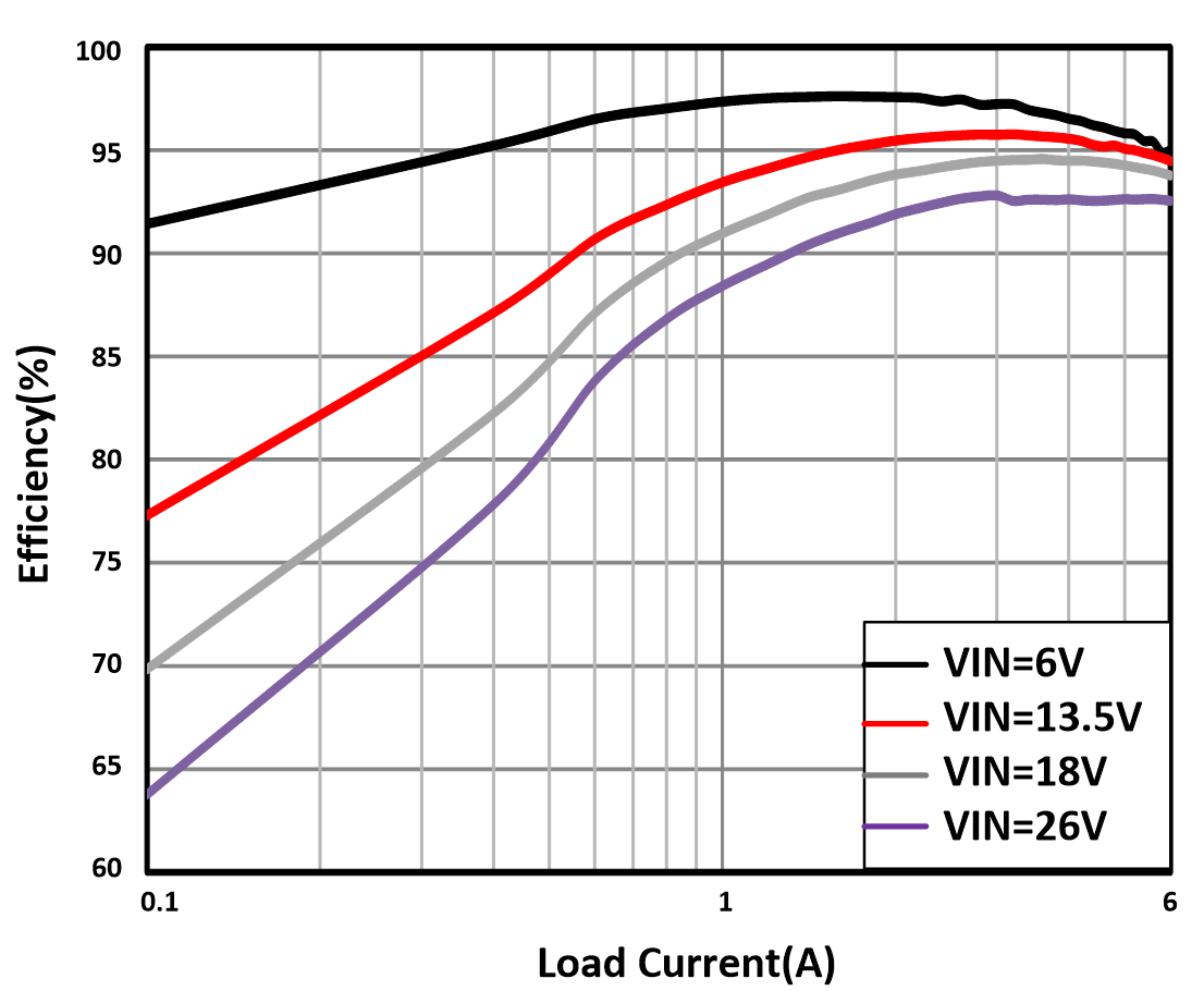
VSET = GND fSW = 400 kHz L = 3.3 uH
Figure 11-2 Buck Only Efficiency. Unless otherwise specified the following conditions apply: VIN = 13.5 V, fSW = 2100 kHz, L = 0.68 µH, CSENSE = 66 µF, CPA_BUS = 1 µF, CPB_BUS = 1 µF, ILIM = GND, TA = 25 °C.
GUID-20210302-CA0I-5F2B-SPBP-FFJQXN57C6NT-low.gif
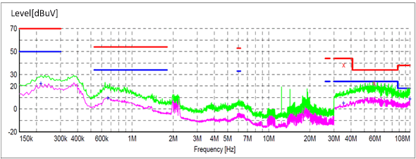
PA_BUS = 3A, PB_BUS = 3A fSW = 2100 kHz L = 0.68 uH
Figure 11-4 2.1-Mhz EMI Results (Without CM Filter)
GUID-20201005-CA0I-T2Q3-JRNJ-C4XFCBB40SNK-low.gif
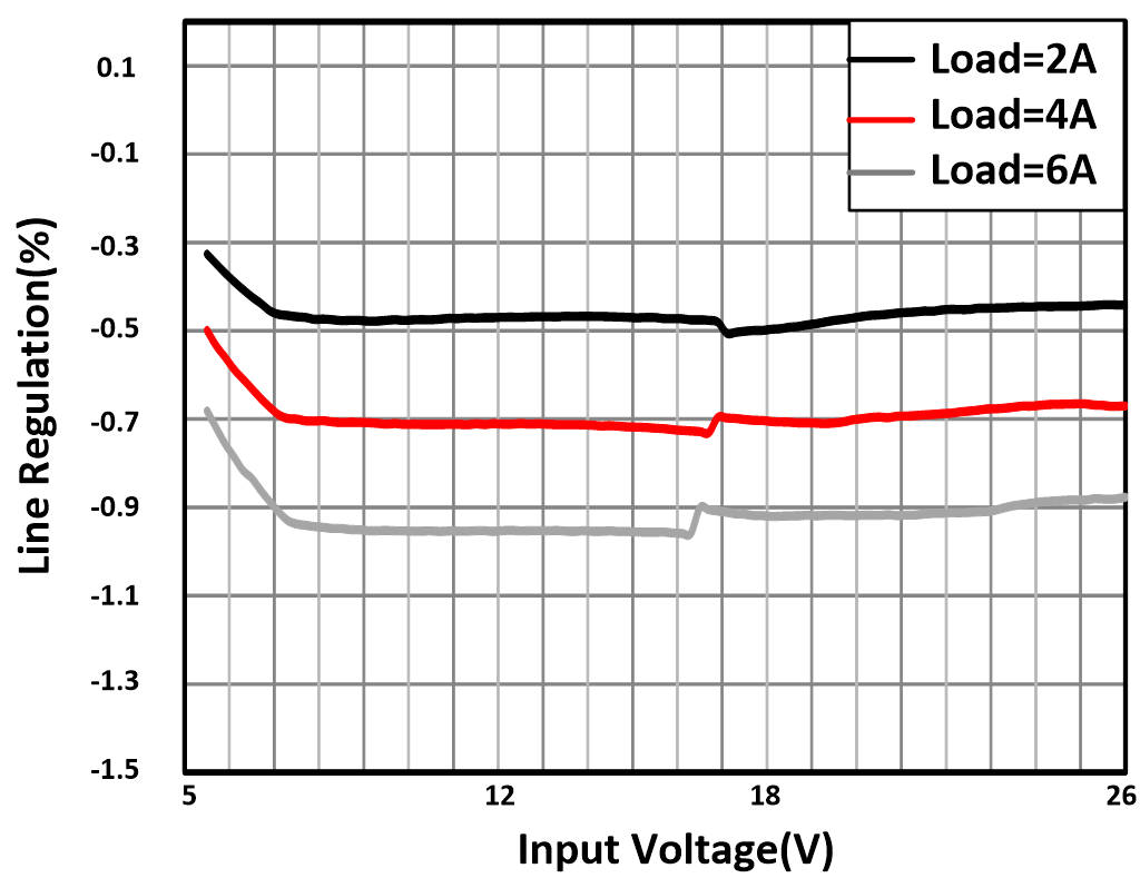
VSET = GND fSW = 2100 kHz
Figure 11-6 Line Regulation
GUID-20201005-CA0I-RHBX-KZK3-D0JP7KB7VHDV-low.gif
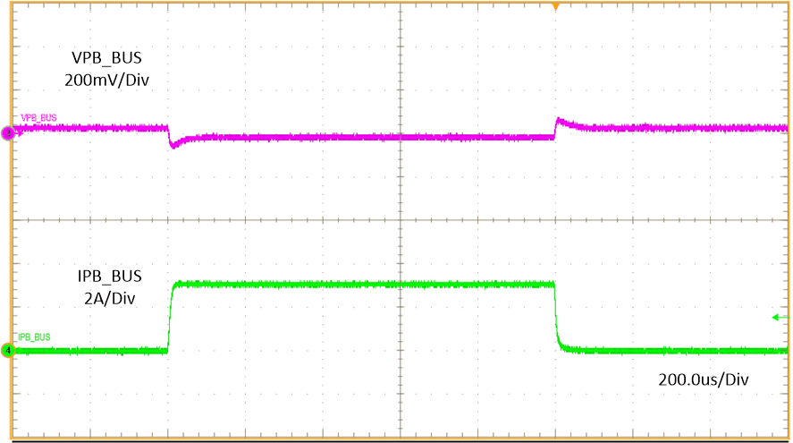
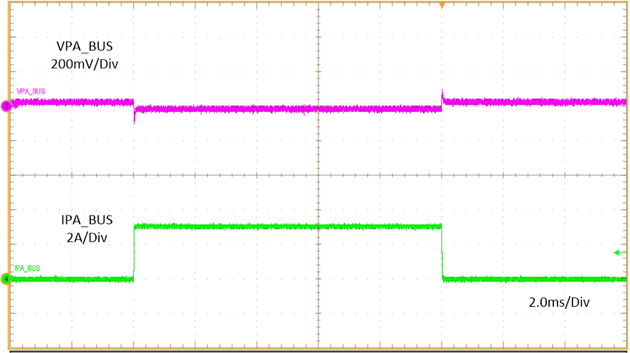
VSET = VSENSE IPB_BUS = 0 A to 3 A IPA_BUS = 3 A fSW = 2100 kHZ
Figure 11-8 Load Transient Without Cable Compensation
GUID-20201005-CA0I-PR4K-9D0S-XWHPFJPR33NH-low.gif
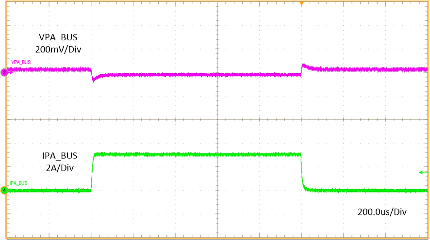
VSET = GND IPA_BUS = 0 A to 3 A IPB_BUS = 3 A fSW = 2100 kHZ
Figure 11-10 Load Transient With Cable Compensation
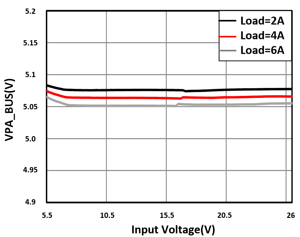
GUID-20201005-CA0I-1BMK-PSVZ-PF0NJQWHF63V-low.gifFigure 11-12 Dropout Characteristic
GUID-20201005-CA0I-XHR9-PNCP-MVMJHQPBLVD3-low.gif
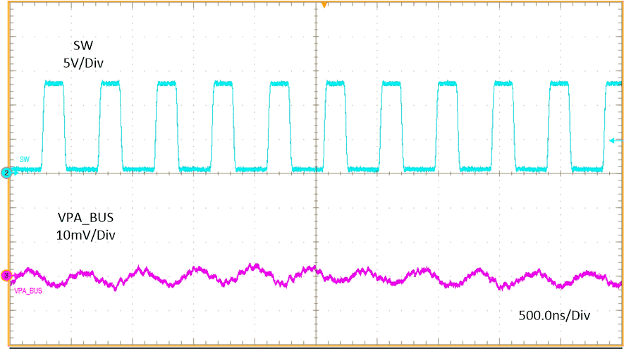
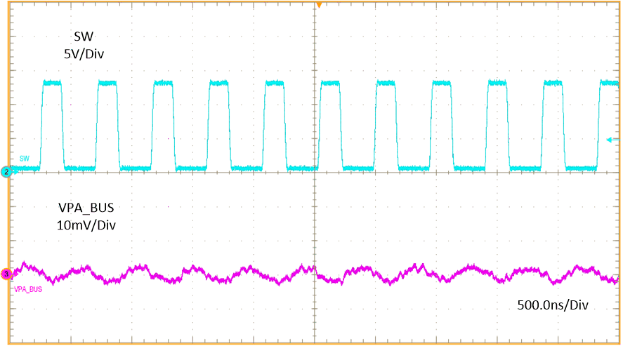
VSET = GND IPA_BUS = 0.1 A IPB_BUS = 0 A fSW = 2100 kHZ
Figure 11-14 100-mA Output Ripple
GUID-20201005-CA0I-ST6S-KJJX-LF30ZD6Z58RF-low.gif
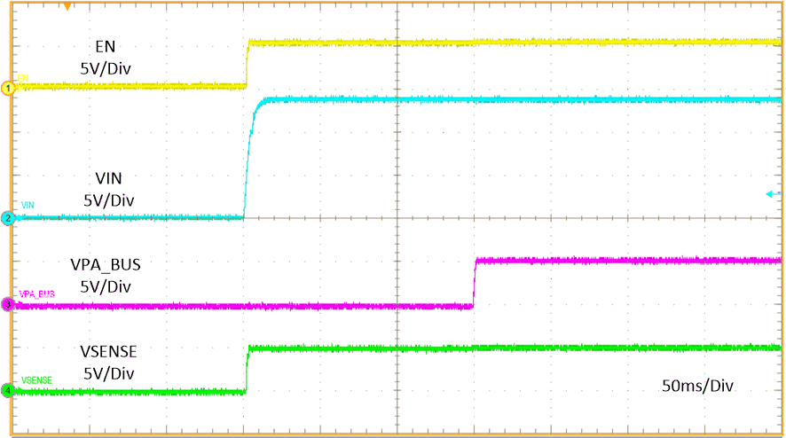
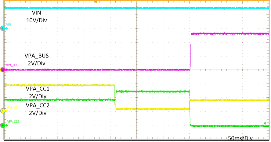
VIN = 0 V to 13.5 V PA_CC1 = Rd IPA_BUS = 3 A
Figure 11-16 Startup Relate to VIN
GUID-20201008-CA0I-DDWQ-RJK4-BXNHXPNJD6WX-low.gif
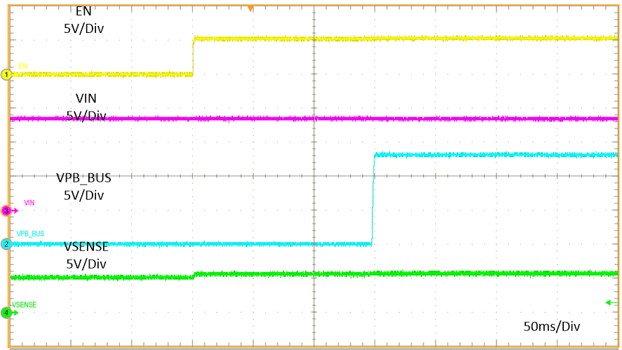
EN = 0 V to 5 V PB_CC1 = Rd IPB_BUS = 3 A
Figure 11-18 Startup Relate to EN
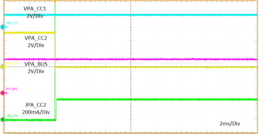
GUID-20201005-CA0I-CTSR-ZX6N-LZWCBB2TMC5P-low.gif
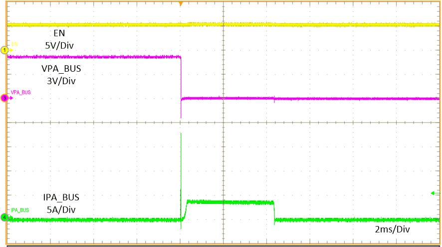
PA_CC1 = Open to Rd PA_CC2 = Open IPA_BUS = 3 A
Figure 11-20 Rd Assert
GUID-20201005-CA0I-LHVM-F9MC-0XWQ4GV6KZHN-low.gif
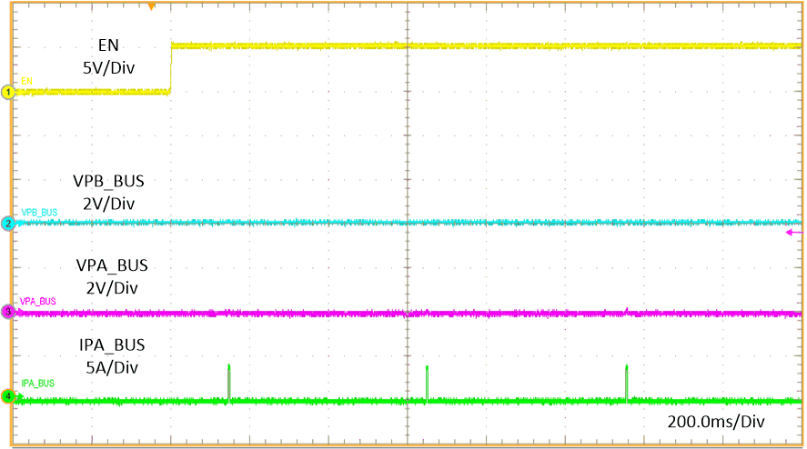
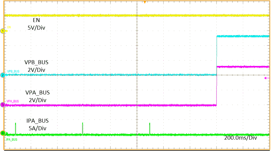
EN to High PA_BUS = GND PB_BUS = GND
Figure 11-22 Enable Into Short
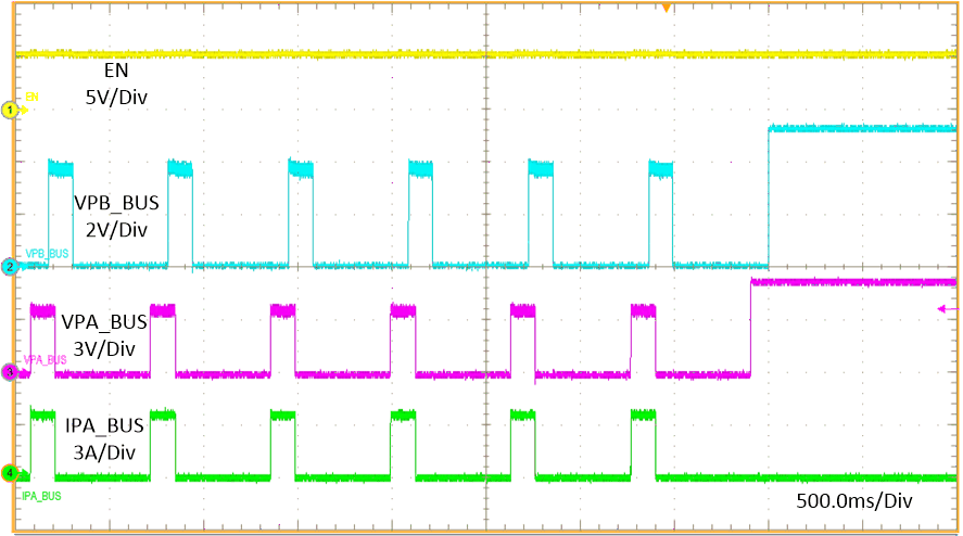
GUID-20201005-CA0I-KZ6H-CQCJ-DHS9SZWMT92P-low.gif
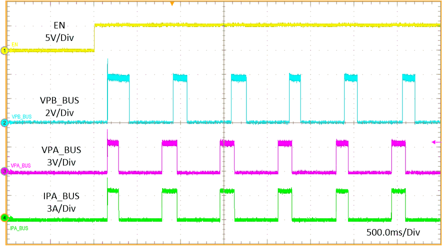
EN to High PA_BUS = 1 Ω PB_BUS = 1 Ω
Figure 11-24 Enable Into 1-Ω Load
GUID-20201005-CA0I-NFRZ-JGQF-HDW4HXMVTKRN-low.gifFigure 11-26 VBUS Hot Short to GND
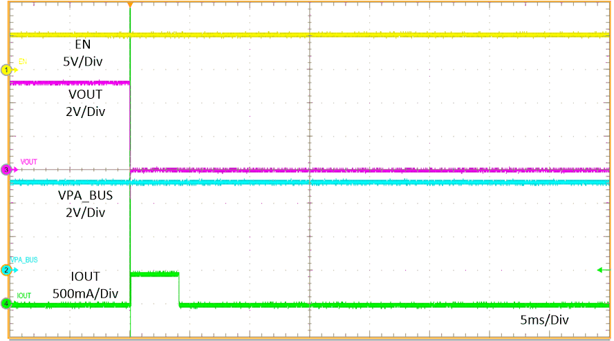
GUID-20201005-CA0I-KMD0-GCXZ-WXGKWMMRMHPG-low.gif
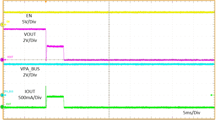
PA_CC1 = Rd OUT = 5.1 Ω PA/B_BUS NO LOAD
Figure 11-28 OUT short to 5.1-Ω Load
GUID-20201005-CA0I-QFNF-CSPV-K301XQD3GZVX-low.gif
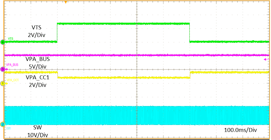
VTS = 0 V to 2.6 V PA_CC1 = Rd PA_CC2 = OPEN
Figure 11-30 Thermal Sensing - NTC Temperature WARM Behavior
GUID-20201005-CA0I-8Z8N-ZK9X-HTP0MPQHHQ28-low.gif
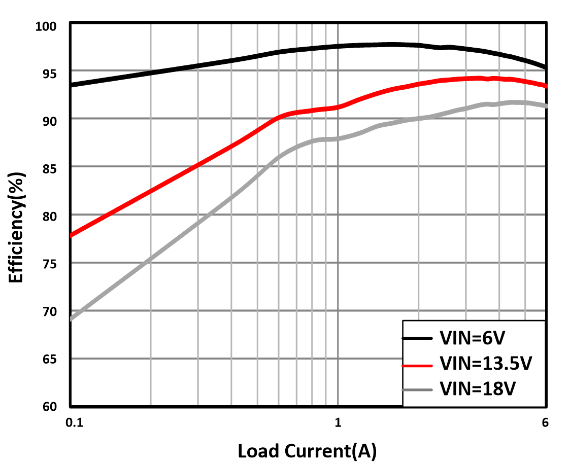
VSET = GND fSW = 2100 kHz L = 0.68 uH
Figure 11-3 Buck Only Efficiency
GUID-20201005-CA0I-DDTX-BWCQ-FPDC0NVK95DD-low.gif
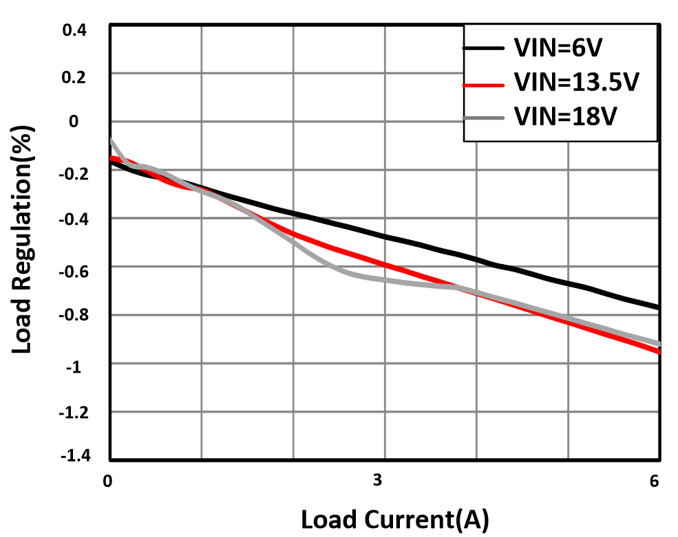
VSET = GND fSW = 2100 kHz
Figure 11-5 Load Regulation
GUID-20201005-CA0I-3F3C-R9LK-HDN5JCK7KK6Z-low.gif
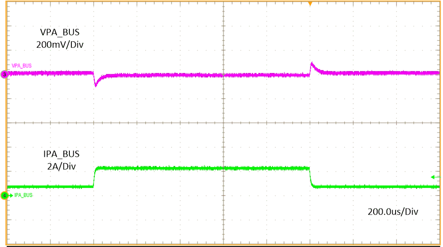
VSET = VSENSE IPA_BUS = 0 A to 3 A IPB_BUS = 3 A fSW = 2100 kHZ
Figure 11-7 Load Transient Without Cable Compensation
GUID-20201005-CA0I-R3JL-5DG0-Q1705MBQRHJK-low.gif
VSET = VSENSE IPA_BUS = 0.75 A to 2.25 A IPB_BUS = 0 A fSW = 400 kHZ
Figure 11-9 Load Transient Without Cable Compensation
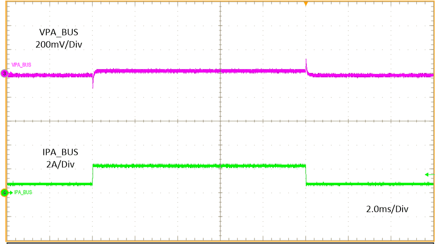
GUID-20201005-CA0I-G2VN-0TRH-MJDRRMQRBM7B-low.gif
VSET = GND IPA_BUS = 0.75 A to 2.25 A IPB_BUS = 0 A fSW = 400 kHZ
Figure 11-11 Load Transient With Cable Compensation
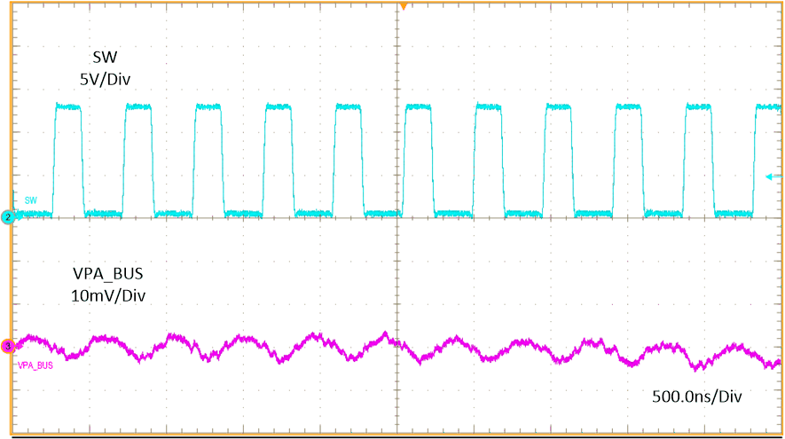
GUID-20201005-CA0I-ZHM5-FSWR-69FMPJVVSDVS-low.gif
VSET = GND IPA_BUS = 3 A IPB_BUS = 3 A fSW = 2100 kHZ
Figure 11-13 6-A Output Ripple
GUID-20201005-CA0I-HWCT-TFTH-JDZMC7SDNZT7-low.gif
VSET = GND IPA_BUS = 0 A IPB_BUS = 0 A fSW = 2100 kHZ
Figure 11-15 No Load Output Ripple
GUID-20201005-CA0I-NRNH-J3KM-TBSDMVGZMC7W-low.gif
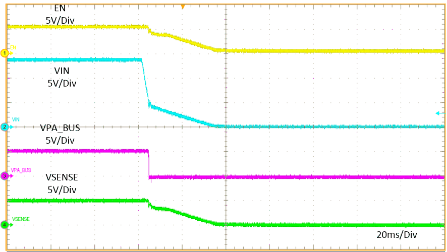
VIN = 13.5 V to 0 V PA_CC1 = Rd IPA_BUS = 3 A
Figure 11-17 Shutdown Relate to VIN
GUID-20201005-CA0I-TJKT-GHHL-VMDJWMSD0K1D-low.gif
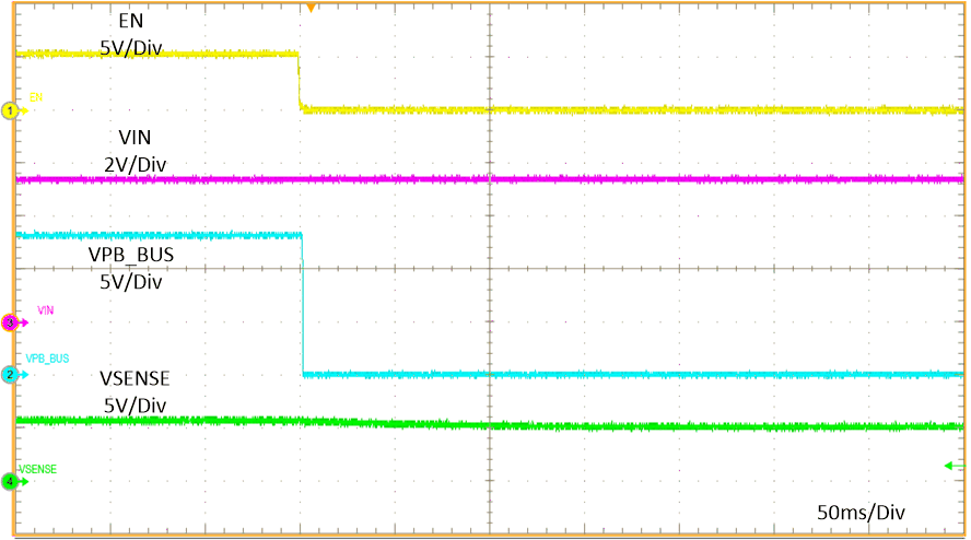
EN = 5 V to 0 V PB_CC1 = Rd IPB_BUS = 3 A
Figure 11-19 Shutdown Relate to EN
GUID-20201005-CA0I-K3XP-QPSS-6RHHV1MQSPDT-low.gif
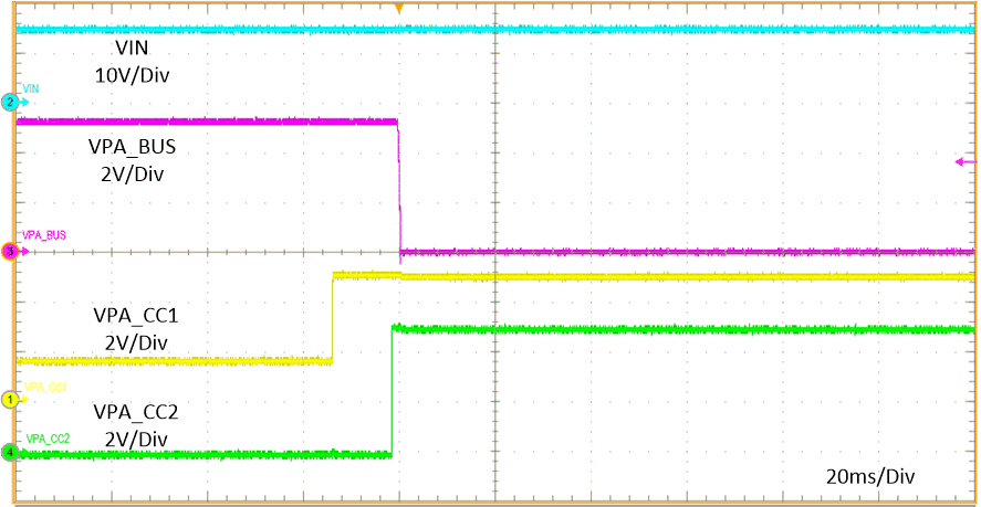
PA_CC1 = Rd to Open PA_CC2 = Open IPA_BUS = 3 A
Figure 11-21 Rd Desert
GUID-20201005-CA0I-BHJW-X5T7-67MJX14GJR3S-low.gifFigure 11-23 Short Circuit Recovery
GUID-20201005-CA0I-KNTL-HKGG-SJDNNZ5KMFRF-low.gifFigure 11-25 1-Ω Load Recovery
GUID-20201005-CA0I-KJPV-RWWX-MFL1GFGRQ7KJ-low.gif
PA_CC1 = Rd PA_CC2 = Ra
Figure 11-27 PA_CC2 Hot Short to GND
GUID-20201005-CA0I-GVNL-GHRB-HTT2QK5FGCST-low.gif
PA_CC1 = Rd OUT = GND PA/B_BUS NO LOAD
Figure 11-29 OUT Hot Short to GND
GUID-20201005-CA0I-1ZQZ-RSZH-LHC1DP03WBSF-low.gif
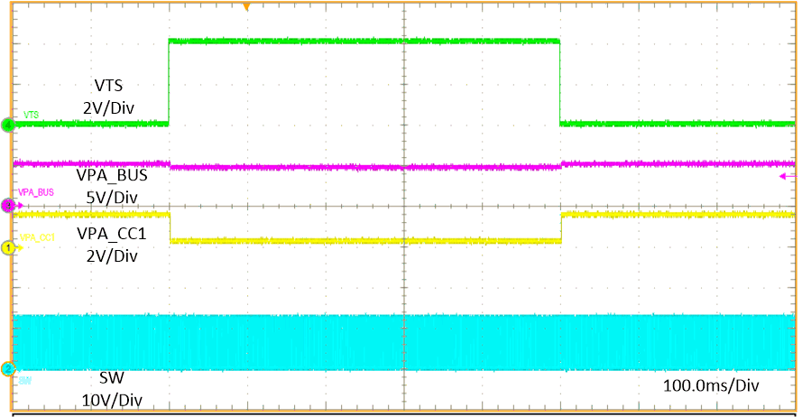
VTS = 0 V to 4 V PA_CC1 = Rd PA_CC2 = OPEN
Figure 11-31 Thermal Sensing - NTC Temperature HOT Behavior