JAJSJU4D May 2020 – September 2021 TPS25850-Q1 , TPS25851-Q1 , TPS25852-Q1
PRODUCTION DATA
- 1 特長
- 2 アプリケーション
- 3 概要
- 4 Revision History
- 5 概要 (続き)
- 6 Device Comparison Table
- 7 Pin Configuration and Functions
- 8 Specifications
- 9 Parameter Measurement Information
-
10Detailed Description
- 10.1 Overview
- 10.2 Functional Block Diagram
- 10.3
Feature Description
- 10.3.1 Power-Down or Undervoltage Lockout
- 10.3.2 Input Overvoltage Protection (OVP) - Continuously Monitored
- 10.3.3 Buck Converter
- 10.3.4 FREQ/SYNC
- 10.3.5 Bootstrap Voltage (BOOT)
- 10.3.6 Minimum ON-Time, Minimum OFF-Time
- 10.3.7 Internal Compensation
- 10.3.8 Selectable Output Voltage (VSET)
- 10.3.9 Current Limit and Short Circuit Protection
- 10.3.10 Cable Compensation
- 10.3.11 Thermal Management With Temperature Sensing (TS) and OTSD
- 10.3.12 Thermal Shutdown
- 10.3.13 USB Enable On/Off Control (TPS25852-Q1)
- 10.3.14 FAULT Indication (TPS25851-Q1 and TPS25852-Q1)
- 10.3.15 USB Specification Overview
- 10.3.16 USB Type-C® Basics
- 10.3.17 USB Port Operating Modes
- 10.4 Device Functional Modes
- 11Application and Implementation
- 12Power Supply Recommendations
- 13Layout
- 14Device and Documentation Support
- 15Mechanical, Packaging, and Orderable Information
10.3.3 Buck Converter
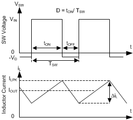
The following operating description of the TPS2585x-Q1 refers to the Functional Block Diagram. The TPS2585x-Q1 integrates a monolithic, synchronous, rectified, step-down, switch-mode converter with internal power MOSFETs and USB current-limit switches with charging ports auto-detection. The TPS2585x-Q1 offers a compact solution that achieves up to 6.6 A of continuous output current with excellent load and line regulation over a wide input supply range. The TPS2585x-Q1 supplies a regulated output voltage by turning on the high-side (HS) and low-side (LS) NMOS switches with controlled duty cycle. During high-side switch ON time, the SW pin voltage swings up to approximately VIN. The inductor current iL increases with linear slope (VIN – VOUT ) / L. When the HS switch is turned off by the control logic, the LS switch is turned on after an anti-shoot-through dead time. Inductor current discharges through the LS switch with a slope of –VOUT / L. The control parameter of a buck converter is defined as Duty Cycle D = tON / TSW, where tON is the high-side switch ON time and TSW is the switching period, shown in Figure 10-2. The regulator control loop maintains a constant output voltage by adjusting the duty cycle D. In an ideal buck converter, where losses are ignored, D is proportional to the output voltage and inversely proportional to the input voltage: D = VOUT / VIN.
 Figure 10-2 SW Node and Inductor Current Waveforms in Continuous Conduction Mode (CCM)
The TPS2585x-Q1 operates in a fixed-frequency, peak-current-mode control to regulate the output voltage. A voltage feedback loop is used to get accurate DC voltage regulation by adjusting the peak current command based on voltage offset. The peak inductor current is sensed from the high-side switch and compared to the peak current threshold to control the ON time of the high-side switch. The voltage feedback loop is internally compensated, which allows for fewer external components, making it easy to design, and provides stable operation with a reasonable combination of output capacitors. The TPS2585x-Q1 operates in FPWM mode for low output voltage ripple, tight output voltage regulation, and constant switching frequency.