JAJSJU4D May 2020 – September 2021 TPS25850-Q1 , TPS25851-Q1 , TPS25852-Q1
PRODUCTION DATA
- 1 特長
- 2 アプリケーション
- 3 概要
- 4 Revision History
- 5 概要 (続き)
- 6 Device Comparison Table
- 7 Pin Configuration and Functions
- 8 Specifications
- 9 Parameter Measurement Information
-
10Detailed Description
- 10.1 Overview
- 10.2 Functional Block Diagram
- 10.3
Feature Description
- 10.3.1 Power-Down or Undervoltage Lockout
- 10.3.2 Input Overvoltage Protection (OVP) - Continuously Monitored
- 10.3.3 Buck Converter
- 10.3.4 FREQ/SYNC
- 10.3.5 Bootstrap Voltage (BOOT)
- 10.3.6 Minimum ON-Time, Minimum OFF-Time
- 10.3.7 Internal Compensation
- 10.3.8 Selectable Output Voltage (VSET)
- 10.3.9 Current Limit and Short Circuit Protection
- 10.3.10 Cable Compensation
- 10.3.11 Thermal Management With Temperature Sensing (TS) and OTSD
- 10.3.12 Thermal Shutdown
- 10.3.13 USB Enable On/Off Control (TPS25852-Q1)
- 10.3.14 FAULT Indication (TPS25851-Q1 and TPS25852-Q1)
- 10.3.15 USB Specification Overview
- 10.3.16 USB Type-C® Basics
- 10.3.17 USB Port Operating Modes
- 10.4 Device Functional Modes
- 11Application and Implementation
- 12Power Supply Recommendations
- 13Layout
- 14Device and Documentation Support
- 15Mechanical, Packaging, and Orderable Information
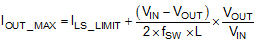
10.3.9.3 Cycle-by-Cycle Buck Current Limit
There is a buck regulator cycle-by-cycle current limit on both the peak and valley of the inductor current.
High-side MOSFET overcurrent protection is implemented by the nature of the peak current mode control. The HS switch current is sensed when the HS is turned on after a set blanking time. The HS switch current is compared to the output of the Error Amplifier (EA) minus slope compensation every switching cycle. The peak current of HS switch is limited by a clamped maximum peak current threshold, IHS_LIMIT, which is constant. The peak current limit of the high-side switch is not affected by the slope compensation and remains constant over the full duty cycle range.
The current going through LS MOSFET is also sensed and monitored. When the LS switch turns on, the inductor current begins to ramp down. The LS switch does not turn OFF at the end of a switching cycle if its current is above the LS current limit, ILS_LIMIT. The LS switch is kept ON so that the inductor current keeps ramping down until the inductor current ramps below the LS current limit, ILS_LIMIT. Then, the LS switch is turned OFF and the HS switch is turned on after a dead time. This action is somewhat different than the more typical peak current limit, and results in Equation 10 for the maximum load current.