JAJSJU4D May 2020 – September 2021 TPS25850-Q1 , TPS25851-Q1 , TPS25852-Q1
PRODUCTION DATA
- 1 特長
- 2 アプリケーション
- 3 概要
- 4 Revision History
- 5 概要 (続き)
- 6 Device Comparison Table
- 7 Pin Configuration and Functions
- 8 Specifications
- 9 Parameter Measurement Information
-
10Detailed Description
- 10.1 Overview
- 10.2 Functional Block Diagram
- 10.3
Feature Description
- 10.3.1 Power-Down or Undervoltage Lockout
- 10.3.2 Input Overvoltage Protection (OVP) - Continuously Monitored
- 10.3.3 Buck Converter
- 10.3.4 FREQ/SYNC
- 10.3.5 Bootstrap Voltage (BOOT)
- 10.3.6 Minimum ON-Time, Minimum OFF-Time
- 10.3.7 Internal Compensation
- 10.3.8 Selectable Output Voltage (VSET)
- 10.3.9 Current Limit and Short Circuit Protection
- 10.3.10 Cable Compensation
- 10.3.11 Thermal Management With Temperature Sensing (TS) and OTSD
- 10.3.12 Thermal Shutdown
- 10.3.13 USB Enable On/Off Control (TPS25852-Q1)
- 10.3.14 FAULT Indication (TPS25851-Q1 and TPS25852-Q1)
- 10.3.15 USB Specification Overview
- 10.3.16 USB Type-C® Basics
- 10.3.17 USB Port Operating Modes
- 10.4 Device Functional Modes
- 11Application and Implementation
- 12Power Supply Recommendations
- 13Layout
- 14Device and Documentation Support
- 15Mechanical, Packaging, and Orderable Information
11.2.2.7 Undervoltage Lockout Set-Point
The system undervoltage lockout (UVLO) is adjusted using the external voltage divider network of RENT and RENB. The UVLO has two thresholds, one for power up when the input voltage is rising and one for power down or brownouts when the input voltage is falling. Equation 13 can be used to determine the VIN UVLO level.
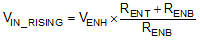
The EN rising threshold (VENH) for the TPS2585x-Q1 is set to be 1.3 V (typical). Choose 10 kΩ for RENB to minimize input current from the supply. If the desired VIN UVLO level is at 6.0 V, then the value of RENT can be calculated using Equation 14:
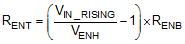
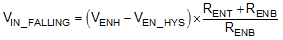
Equation 14 yields a value of 36.1 kΩ. The resulting falling UVLO threshold equals 5.5 V and can be calculated by Equation 15, where EN hysteresis (VEN_HYS) is 0.1 V (typical).
Note that it cannot connect EN to IN pin directly for self-start up. Because the voltage rating of EN pin is 11 V, tying it to VIN directly damages the device. The simplest way to enable the operation of the TPS2585x-Q1 is to connect the EN to VSENSE. This connection allows the automatic start up when VIN is within the operation range.