JAJSF90F October   2017  – December 2021 TPS2662

PRODUCTION DATA  

  1. 特長
  2. アプリケーション
  3. 概要
  4. Revision History
  5. Device Comparison Table
  6. Pin Configuration and Functions
  7. Specifications
    1. 7.1 Absolute Maximum Ratings
    2. 7.2 ESD Ratings
    3. 7.3 Recommended Operating Conditions
    4. 7.4 Thermal Information
    5. 7.5 Electrical Characteristics
    6. 7.6 Timing Requirements
    7. 7.7 Typical Characteristics
  8. Parameter Measurement Information
  9. Detailed Description
    1. 9.1 Overview
    2. 9.2 Functional Block Diagram
    3. 9.3 Feature Description
      1. 9.3.1 Undervoltage Lockout (UVLO)
      2. 9.3.2 Overvoltage Protection (OVP)
      3. 9.3.3 Hot Plug-In and Inrush Current Control
      4. 9.3.4 Reverse Polarity Protection
        1. 9.3.4.1 Input Side Reverse Polarity Protection
        2. 9.3.4.2 Output Side Reverse Polarity Protection
      5. 9.3.5 Overload and Short-Circuit Protection
        1. 9.3.5.1 Overload Protection
        2.       28
        3. 9.3.5.2 Short-Circuit Protection
          1. 9.3.5.2.1 Start-Up With Short-Circuit On Output
      6. 9.3.6 Reverse Current Protection
      7. 9.3.7 FAULT Response
      8. 9.3.8 IN, OUT, RTN, and GND Pins
      9. 9.3.9 Thermal Shutdown
    4. 9.4 Device Functional Modes
      1. 9.4.1 Low Current Shutdown Control (SHDN)
  10. 10Application and Implementation
    1. 10.1 Application Information
    2. 10.2 Typical Application
      1. 10.2.1 Design Requirements
      2. 10.2.2 Detailed Design Procedure
        1. 10.2.2.1 Step-by-Step Design Procedure
        2. 10.2.2.2 Programming the Current Limit Threshold R(ILIM) Selection
        3. 10.2.2.3 Undervoltage Lockout and Overvoltage Set Point
        4. 10.2.2.4 Setting Output Voltage Ramp Time—(tdVdT)
          1. 10.2.2.4.1 Case 1: Start-Up Without Load—Only Output Capacitance C(OUT) Draws Current During Start-Up
          2. 10.2.2.4.2 Case 2: Start-Up With Load —Output Capacitance C(OUT) and Load Draws Current During Start-Up
          3. 10.2.2.4.3 Support Component Selections – R FLT and C(IN)
      3. 10.2.3 Application Curves
    3. 10.3 System Examples
      1. 10.3.1 Field Supply Protection in PLC, DCS I/O Modules
      2. 10.3.2 Simple 24-V Power Supply Path Protection
      3. 10.3.3 Power Stealing in Smart Thermostat
    4. 10.4 Do's and Don'ts
  11. 11Power Supply Recommendations
    1. 11.1 Transient Protection
  12. 12Layout
    1. 12.1 Layout Guidelines
    2. 12.2 Layout Example
  13. 13Device and Documentation Support
    1. 13.1 Documentation Support
      1. 13.1.1 Related Documentation
    2. 13.2 Receiving Notification of Documentation Updates
    3. 13.3 サポート・リソース
    4. 13.4 Trademarks
    5. 13.5 Electrostatic Discharge Caution
    6. 13.6 Glossary
  14. 14Mechanical, Packaging, and Orderable Information

パッケージ・オプション

メカニカル・データ(パッケージ|ピン)
サーマルパッド・メカニカル・データ
発注情報

IN, OUT, RTN, and GND Pins

TI recommends a ceramic bypass capacitor close to the device from IN to GND to alleviate bus transients. The recommended input operating voltage range is 4.5 to 60 V. V(OUT), in the ON condition, is calculated using Equation 4.
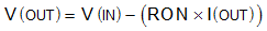
Equation 4. GUID-68035FBF-A140-4DAB-9502-30F1189C42AA-low.gif

Where,

  • RON is the total ON resistance of the internal FETs.

GND pin must be connected to the system ground. RTN is the device ground reference for all the internal control blocks. Connect the TPS2662x family support components: R(ILIM), C(dVdT) and resistors for UVLO and OVP with respect to the RTN pin. Internally, the device has reverse input polarity protection block between RTN and the GND terminal. Connecting RTN pin to GND pin disables the reverse polarity protection feature and the TPS2662x gets permanently damaged when operated under this fault event.