JAJSF90F October 2017 – December 2021 TPS2662
PRODUCTION DATA
- 1 特長
- 2 アプリケーション
- 3 概要
- 4 Revision History
- 5 Device Comparison Table
- 6 Pin Configuration and Functions
- 7 Specifications
- 8 Parameter Measurement Information
-
9 Detailed Description
- 9.1 Overview
- 9.2 Functional Block Diagram
- 9.3
Feature Description
- 9.3.1 Undervoltage Lockout (UVLO)
- 9.3.2 Overvoltage Protection (OVP)
- 9.3.3 Hot Plug-In and Inrush Current Control
- 9.3.4 Reverse Polarity Protection
- 9.3.5 Overload and Short-Circuit Protection
- 9.3.6 Reverse Current Protection
- 9.3.7 FAULT Response
- 9.3.8 IN, OUT, RTN, and GND Pins
- 9.3.9 Thermal Shutdown
- 9.4 Device Functional Modes
-
10Application and Implementation
- 10.1 Application Information
- 10.2 Typical Application
- 10.3 System Examples
- 10.4 Do's and Don'ts
- 11Power Supply Recommendations
- 12Layout
- 13Device and Documentation Support
- 14Mechanical, Packaging, and Orderable Information
パッケージ・オプション
メカニカル・データ(パッケージ|ピン)
- DRC|10
サーマルパッド・メカニカル・データ
- DRC|10
発注情報
10.2.2.3 Undervoltage Lockout and Overvoltage Set Point
The undervoltage lockout (UVLO) and overvoltage trip point are adjusted using an external voltage divider network of R1, R2 and R3 connected between IN, UVLO, OVP and RTN pins of the device. The values required for setting the undervoltage and overvoltage are calculated by solving Equation 6 and Equation 7.
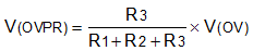
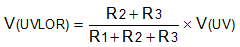
For minimizing the input current drawn from the power supply {I(R123) = V(IN) / (R1+R2+R3)}, TI recommends to use higher value resistance for R1, R2 and R3.
However, the leakage current due to external active components connected at resistor string can add error to these calculations. So, the resistor string current, I(R123) must be chosen to be 20 times greater than the leakage current of UVLO and OVP pins.
From the device electrical specifications, V(OVPR) = 1.19 V and V(UVLOR) = 1.19 V. From the design requirements, V(OV) is 30 V and V(UV) is 18 V. To solve the equation, first choose the value of R3 = 30.1 kΩ and use Equation 6 to solve for (R1 + R2) = 728.7 kΩ. Use Equation 7 and value of (R1 + R2) to solve for R2 = 20.05 kΩ and finally R1= 708.6 kΩ.
Choose the closest standard 1% resistor values: R1 = 715 kΩ, R2 = 20 kΩ, and R3 = 30.1 kΩ.