JAJSGA2F September 2018 – June 2021 TPS2663
PRODUCTION DATA
- 1 特長
- 2 アプリケーション
- 3 概要
- 4 Revision History
- 5 Device Comparison Table
- 6 Pin Configuration and Functions
- 7 Specifications
- 8 Parameter Measurement Information
-
9 Detailed Description
- 9.1 Overview
- 9.2 Functional Block Diagram
- 9.3
Feature Description
- 9.3.1 Hot Plug-In and In-Rush Current Control
- 9.3.2 PGOOD and PGTH
- 9.3.3 Undervoltage Lockout (UVLO)
- 9.3.4 Overvoltage Protection (OVP)
- 9.3.5 Input Reverse Polarity Protection (B_GATE, DRV)
- 9.3.6 Reverse Current Protection
- 9.3.7 Overload and Short Circuit Protection
- 9.3.8 Output Power Limiting, PLIM (TPS26632, TPS26633, TPS26635 and TPS26636 Only)
- 9.3.9 Current Monitoring Output (IMON)
- 9.3.10 FAULT Response ( FLT)
- 9.3.11 IN_SYS, IN, OUT and GND Pins
- 9.3.12 Thermal Shutdown
- 9.3.13 Low Current Shutdown Control (SHDN)
- 9.4 Device Functional Modes
-
10Application and Implementation
- 10.1 Application Information
- 10.2
Typical Application: Power Path Protection in a PLC System
- 10.2.1 Design Requirements
- 10.2.2 Detailed Design Procedure
- 10.2.3 Application Curves
- 10.3 System Examples
- 10.4 Do's and Don'ts
- 11Power Supply Recommendations
- 12Layout
- 13Device and Documentation Support
- 14Mechanical, Packaging, and Orderable Information
9.3.5 Input Reverse Polarity Protection (B_GATE, DRV)
The TPS2663x devices support the reverse input
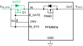
polarity protection feature. Connect an N-channel power FET (Q1) with the source to
IN_SYS, drain to IN and GATE to B-GATE as shown in Figure 9-5. This forms a back to back FET topology in power path that is required to protect
the load from input reverse polarity faults. Connect an external signal FET (Q2)
across BGATE, DRV and IN_SYS. Q2 acts as a pull down gate switch for Q1. In the
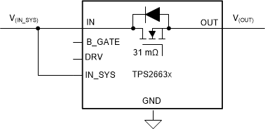
applications where reverse polarity protection and reverse current blocking is not
required then connect IN_SYS and IN together. Leave BGATE and DRV open as shown in
Figure 9-6.
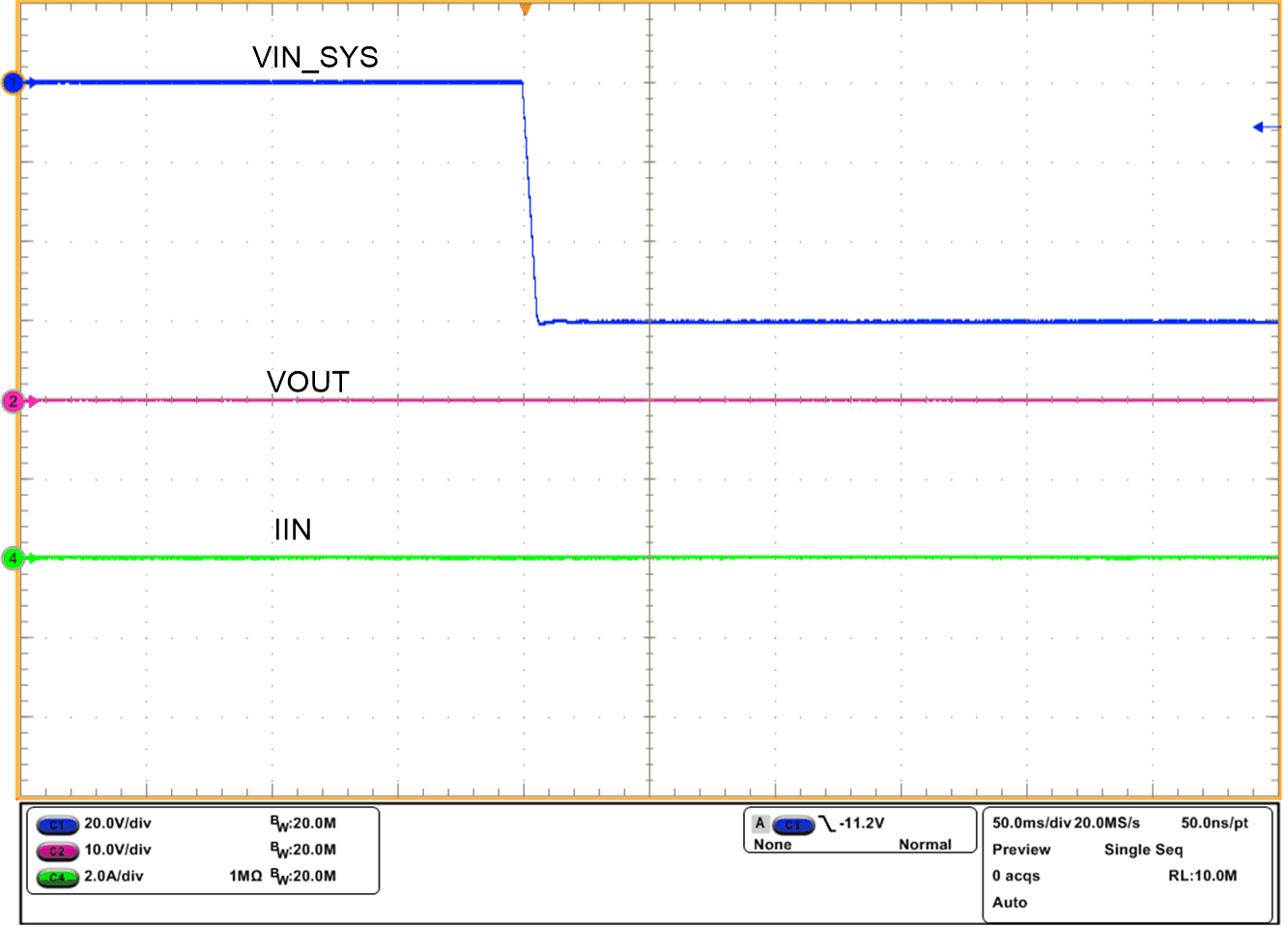
Figure 8-7 illustrates the reverse input polarity protection
functionality.
The TPS2663x devices support a maximum differential voltage across V(IN_SYS) – V(OUT) upto –85 V. This high voltage transients generally appear during the IEC61000-4-5 surge testing at the V(IN_SYS). This voltage stress appears across the external N-channel FET. The TPS2663x provides a gate drive (B_GATE) of 10.2 V (typical). The fast pull down gate switch Q2 pulls down the GATE of the Q1 during reverse current and reverse polarity fault events. Q2 should be at least 15-V, VDS rated FET with a maximum VGS rating of 20-V, Ciss ≤ 50 pF and VGTH(min) ≤ 3 V.


